S-25C040A0H-K8T2UD EEPROM: Full Pinout, Timings & Specs
The S-25C040A0H-K8T2UD is a 4-Kbit serial SPI EEPROM typically organized as 512 × 8 for small non-volatile parameter and calibration storage. Designers need capacity class, interface type, VCC range and page/write timing before layout. These figures are specified in the official datasheet (see Device Overview and Electrical Characteristics). This article compiles pinout, timing, electrical and implementation checklists into a single reference for embedded engineers.
Our purpose is to provide a compact, actionable integration guide for hardware designers and firmware engineers. The focus is placed on pinout, recommended wiring, timing parameters and debug flows. Recommended wiring and timing behavior follow the official datasheet timing diagrams and command descriptions. Follow the tables and checklists here as an integration checklist and always confirm exact numeric values on the official datasheet prior to production.
1 — Device overview & quick specs
The S-25C040A0H-K8T2UD is a 4-Kbit SPI EEPROM device suitable for byte- and page-oriented operations. Capacity, interface and operating ranges are defined in the datasheet. Use the part-number cues below to interpret capacity, package and grade and verify the one-line spec table for VCC, max clock, page size and endurance before committing to a design.
1.1 Part-number breakdown & what the suffixes imply
Interpreting the part number reduces ordering mistakes. Typical segment meanings are documented in the datasheet ordering info. A common breakdown is:
- S-25C040 — Family & 4-Kbit density (512 words × 8-bit)
- A0H — Internal revision/feature flag and high temperature operation class
- K8T2UD style — Packaging, pin count, and environmental qualification code
1.2 One-page spec-at-a-glance table
This consolidated table maps out key design boundaries based on standard operating conditions:
| Parameter | Datasheet Standard Value | Test Conditions / Notes |
|---|---|---|
| Memory organization | 4 Kbit (512 × 8) | Byte-addressable array |
| Interface | SPI (Mode 0 & Mode 3 compatible) | SI, SO, SCK, CS |
| VCC range | 1.6 V to 5.5 V | Full industrial supply range |
| Max clock (fSCK) | 5.0 MHz (2.5V to 5.5V) / 2.0 MHz (< 2.5V) | TA = -40°C to +85°C |
| Page size | 16 Bytes | Page-write boundary limits |
| Write cycle (tWC) | 4.0 ms (Max) | Self-timed write cycle |
| Endurance / Retention | 10^6 cycles / 100 years | At nominal operating temperature |
2 — Full pinout & pin functions
Correct pin mapping and polarity are critical to avoiding bus conflicts. Pin assignments and recommended pull values are listed in the official datasheet pin descriptions. Below are practical mapping and wiring recommendations—use the datasheet package drawings to confirm land pattern and pin 1 orientation.
2.1 Pin diagrams by package + mapping table
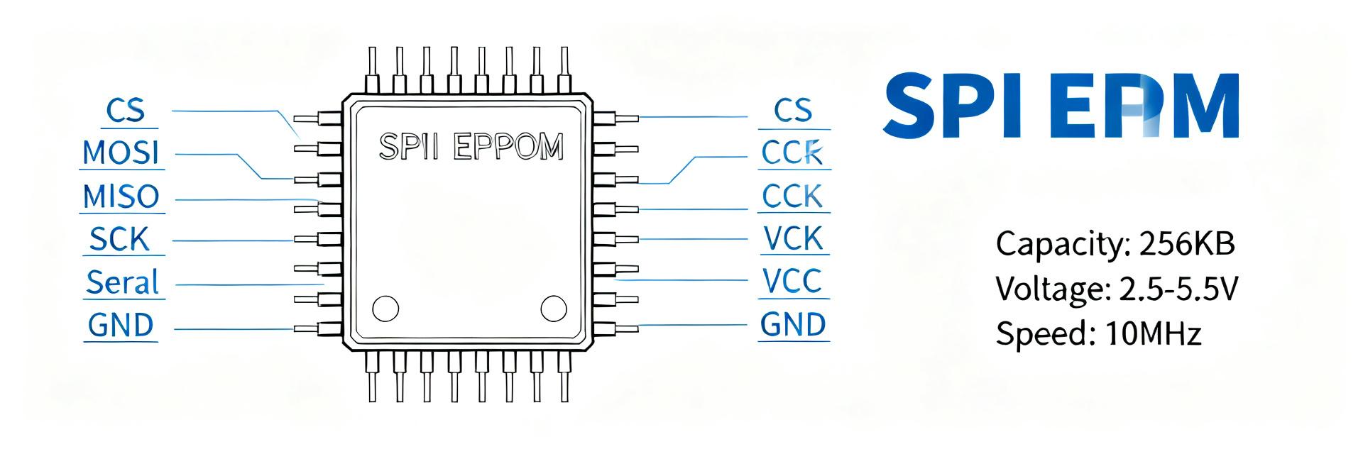
Package variants map pins consistently. The pin names are standard for SPI EEPROMs: CS (Chip Select), SCK, SI (MOSI), SO (MISO), WP, HOLD, VCC, GND. The table below provides the generic pin-to-function map:
| Pin # | Name | Function | I/O Type |
|---|---|---|---|
| 1 | CS | Chip select, active low | Input |
| 2 | SO | Serial data out (MISO) | Output (Tri-state) |
| 3 | WP | Write protect (active low) | Input |
| 4 | GND | Ground reference | Power |
| 5 | SI | Serial data in (MOSI) | Input |
| 6 | SCK | Serial clock input | Input |
| 7 | HOLD | Pause serial I/O when asserted low | Input |
| 8 | VCC | Supply Voltage input | Power |
2.2 Pin-level usage notes & recommended external components
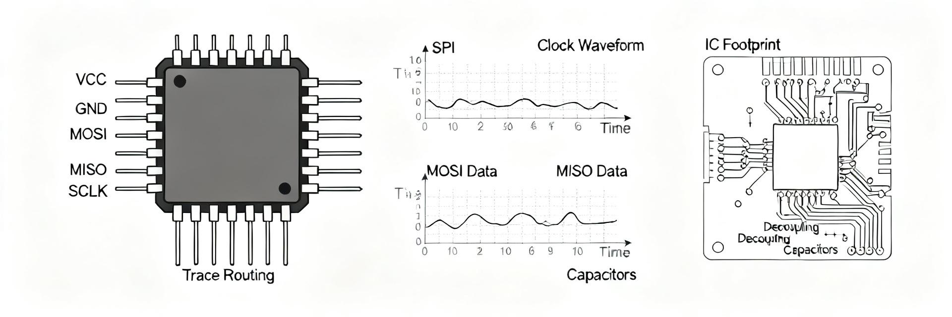
Recommended external components reduce noise and protect the bus. Typical wiring involves placing a 0.1 µF decoupling capacitor close to VCC and GND pins. Use 10 kΩ pull-up resistors on CS if idle-high, series 22–100 Ω resistors on SCK/SI/SO for ringing control, and 10 kΩ pull-ups or driven high states for WP/HOLD to prevent state floating.
3 — Timings, protocol & example transactions
Correct CPOL/CPHA and adherence to timing parameters prevents corrupt writes. Timing parameters (such as setup/hold, clock high/low times, and write cycles) are defined in the official datasheet. Use the datasheet timing table as the authoritative source; below are protocol notes and example sequences.
3.1 SPI timing parameters & timing diagram guidance
Ensure correct timing margins are maintained during physical validation. The SPI bus supports both standard Mode 0 (0,0) and Mode 3 (1,1). Ensure the microcontroller SPI clock rate is scaled properly to match the maximum frequency relative to your layout's current VCC level (e.g. limit fSCK to 2.0 MHz if operating below 2.5V).
3.2 Command set summary & example SPI sequences
Write operations require executing a Write Enable (WREN) command before sending data, followed by polling the status register (RDSR) until write-in-progress (WIP) transitions back to 0. Use the following operations:
- WREN (0x06): Sets the write enable latch.
- WRITE (0x02): Followed by 8-bit address (for 4-Kbit limits) and data bytes.
- READ (0x03): Followed by 8-bit address to read continuous stream.
- RDSR (0x05): Reads the status register to poll the WIP bit.
4 — Electrical characteristics & reliability considerations
Power and leakage characteristics influence standby budgets. Include test conditions (VCC, TA) when logging values. Plan decoupling and power sequencing and watch for hot-plug limitations documented in the datasheet.
4.1 Supply, currents, voltage thresholds & power modes
Active and standby currents must be verified for battery-backed or low-power designs. Standby current is typically in the microamp range when CS is pulled high to VCC. Maintain proper power ramping thresholds to allow internal power-on-reset (POR) circuits to initialize state parameters reliably.
4.2 Endurance, data retention, write protection & ESD
Endurance and retention determine your system lifecycle strategy. Hardware write protection is enabled dynamically by pulling WP low in combination with status register write disable settings. For high-frequency write architectures, wear-leveling algorithms in the host MCU are recommended to maximize active lifespan.
5 — Implementation, PCB footprint & troubleshooting
Correct footprint and layout reduce EMI and signal integrity issues. Place decoupling capacitors next to the VCC pin, keep SPI traces short, use ground planes, orient the pin 1 marker clearly, and reserve space for series resistors and pull components.
5.1 PCB footprint, layout best practices & reference schematics
Ensure the copper land pads match the target package (e.g., SNT-8A, SOP-8). Do not route high-speed signals or noisy switching rails directly beneath the EEPROM package. Pull-up configurations must be sized to accommodate rise-time limits at faster clock ranges.
5.2 Common failure modes, test procedures & debugging checklist
Common issues include wrong CPOL/CPHA, WP asserted, HOLD floating, and bus contention. Check these vectors during hardware review:
- Verify VCC supply levels and decoupling caps right at the pins.
- Probe CS, SCK, SI, and SO with an oscilloscope to confirm proper signal transitions.
- Check that the HOLD and WP pins are not floating or unexpectedly driven low.
- Ensure the host controller polls the WIP bit of the status register before sending subsequent write commands.
Conclusion / Summary
This consolidated reference highlights the integration-critical items for the S-25C040A0H-K8T2UD. Always confirm electrical and timing numbers from the official datasheet before production and use the tables and checklists above as an integration checklist to reduce rework.
Key Summary
- Confirm S-25C040A0H-K8T2UD exact VCC, max clock, page size and tWC in the official datasheet before layout; use the spec table above as a template for documentation.
- Pinout: CS (active low), SCK, SI (MOSI), SO (MISO), WP and HOLD require defined pull or GPIO control; place decoupling close to VCC to protect I/O integrity.
- Timing & protocol: implement WREN before writes, poll RDSR for WIP, and set MCU SPI CPOL/CPHA per the datasheet timing diagrams to avoid corrupted transfers.
Common Questions
What is the pinout configuration for S-25C040A0H-K8T2UD?
The S-25C040A0H-K8T2UD SPI EEPROM features a standard 8-pin layout: Pin 1 is CS (Chip Select, active low), Pin 2 is SO (Serial Output / MISO), Pin 3 is WP (Write Protect, active low), Pin 4 is GND, Pin 5 is SI (Serial Input / MOSI), Pin 6 is SCK (Serial Clock), Pin 7 is HOLD (Suspends serial transmission, active low), and Pin 8 is VCC. Double-check physical pin mapping against your specific package mechanical footprint.
What are the write timings and polling methods recommended for this EEPROM?
To write data, first send a Write Enable (WREN) command, then issue the WRITE instruction with address and data bytes. The physical write cycle (tWC) takes a maximum of 4.0 ms. Instead of implementing a blind wait delay, it is highly recommended to dynamically poll the Status Register using the Read Status Register (RDSR) command. Monitor the Write In Progress (WIP) bit (Bit 0) until it returns to 0 to minimize latency.
What are the electrical characteristics (VCC and clock frequency) of S-25C040A?
The S-25C040A0H operates across a wide supply voltage (VCC) range from 1.6V to 5.5V. Its maximum serial clock frequency (fSCK) varies with supply voltage: up to 5.0 MHz in the 2.5V to 5.5V range, and up to 2.0 MHz in the 1.6V to 2.5V range. Standby current is minimized to under 1.0 uA under standard test conditions.
How can I troubleshoot communication and write issues with the SPI interface?
First, measure VCC stability and verify that a 0.1 uF decoupling capacitor is placed close to the chip pins. Verify that CS toggles correctly per SPI transaction and that CPOL/CPHA settings conform to Mode 0 (0,0) or Mode 3 (1,1). Ensure the WP and HOLD pins are tied securely to VCC or active GPIO outputs to prevent unexpected state changes, and capture bus lines with a logic analyzer to verify the WREN sequence before write attempts.