S-8520E30MC-BJPNT2G Datasheet: Pinout & Electrical Specs
The manufacturer datasheet lists this device as a voltage‑mode step‑down switching controller with a maximum switching frequency around 300 kHz and quiescent/current‑sense behavior suitable for low‑current DC‑DC designs — making it a common choice for compact power rails in embedded systems. This guide breaks the S-8520E30MC-BJPNT2G datasheet into practical pinout, electrical specs, limits, layout and integration guidance so engineers can make design decisions quickly and confidently.
Background: What the S-8520E30MC-BJPNT2G Is
The S-8520E30MC-BJPNT2G is a voltage‑mode buck (step‑down) switching controller intended for small embedded power rails and low‑power converters. It targets designers needing compact controllers with moderate switching frequency and straightforward external component selection. The device typically ships in a small PDSO‑5 style package and is optimized for efficiency and minimal external parts count.
Device class & core function
This controller implements voltage‑mode PWM regulation: it compares feedback voltage to an internal reference and drives an external switch to maintain VOUT. Key numeric highlight from the datasheet is a switching frequency near 300 kHz, which balances component size and EMI. Typical uses include microcontroller rails, sensor supplies, and small point‑of‑load converters; the S-8520E30MC-BJPNT2G datasheet is the authoritative reference for exact electrical limits and recommended conditions.
Key terms and how to read this datasheet
Essential terms: VIN (input supply), VOUT (regulated output), SW node (switching node between switch and catch diode/inductor), EN/SHDN (enable or shutdown pin), FB (feedback), OSC (oscillator/frequency control), quiescent current (no‑load supply current), and thermal resistance (junction‑to‑ambient). Datasheets separate Absolute Maximum Ratings (limits you must never exceed) and Recommended Operating Conditions (guaranteed performance region) — use both when validating margins and derating.
Pinout & Mechanical Details
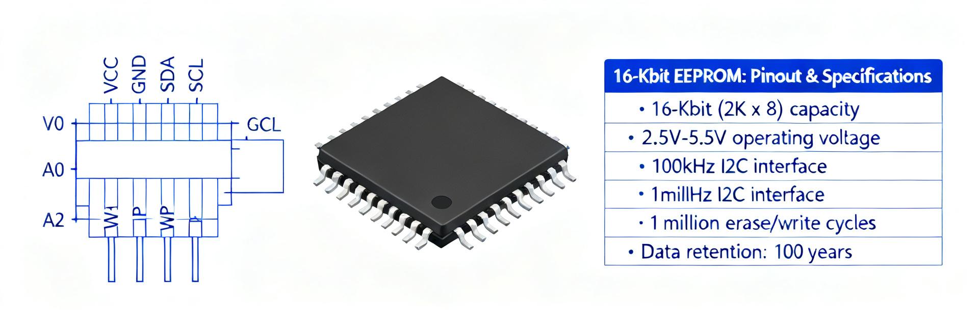
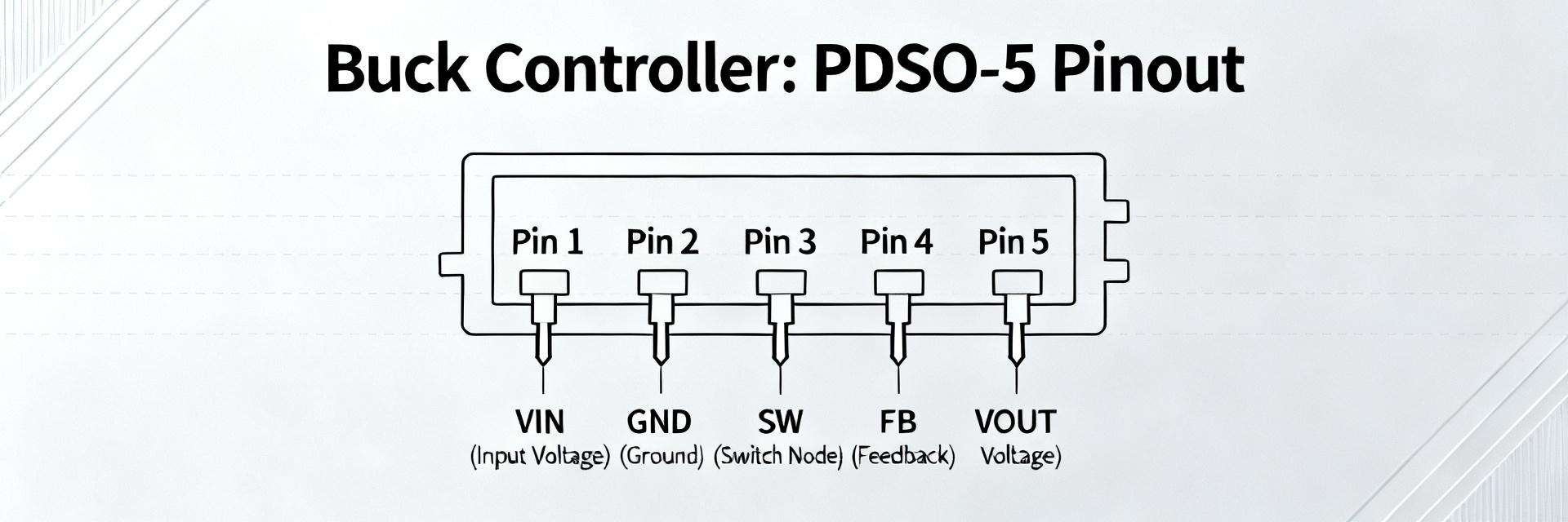
The package is compact and typically has five functional pins plus a thermal pad. Pay attention to recommended land pattern, thermal pad soldering, and solder mask openings; mechanical tolerances affect reflow yield and thermal performance. Below is a concise pin table template and practical PCB connection guidance to match the datasheet pin functions and routing best practices.
Pin-by-pin breakdown (pinout)
Use this table as the canonical mapping from pin number to role and recommended PCB connection; adapt actual names to the datasheet diagram in your copy of the datasheet.
| Pin # | Pin Name | Function | Typical PCB Connection |
|---|---|---|---|
| 1 | VIN | Input supply; powers internal circuits | Close to input decoupling cap, short trace to thermal/power vias |
| 2 | SW | Switch node (to inductor/catch diode) | Keep short; isolate ring; avoid runs near FB |
| 3 | GND | Signal and power return | Connect to ground plane with via array |
| 4 | FB | Feedback input for regulation | Short, single‑trace route to divider, away from SW noise |
| 5 | EN / OSC | Enable or frequency control | Pull high/low via resistor; bypass with small cap if recommended |
Package, footprint, and mounting notes
Follow the datasheet land pattern: maximize copper under thermal pad, add thermal vias to inner or bottom plane, and use controlled solder mask openings. Typical tolerances require 0.05 mm pad adjustments per fab notes; keep the switch node exposed copper areas minimized to reduce EMI. A solid ground plane and stitched vias under the thermal pad improve thermal dissipation and reliability.
Electrical Specifications & Limits
Designers should extract key electrical specs early: VIN range, reference/FB thresholds, quiescent current, switch characteristics, and thermal resistances. Use the datasheet test conditions when comparing typical vs guaranteed values to ensure a robust design across temperature and production variation.
DC electrical specs (recommended operating conditions)
Important electrical specs include the approximate switching frequency (~300 kHz), the internal reference used for regulation, and the device's quiescent current behavior that makes it suitable for low‑current converters. Interpreting typical vs guaranteed values: "typical" reflects characterization at specific Ta and test conditions; "min/max" are guaranteed over the recommended operating range and should be used for worst‑case margin calculations when designing supplies.
Absolute maximum ratings & thermal limits
Absolute maxima cover maximum VIN, maximum SW node voltage, junction temperature (Tj), storage temperature, and ESD class. Always leave headroom between operating VIN and absolute max VIN and derate power dissipation based on package thermal resistance. Use thermal vias and copper pour to reduce junction rise; validate with worst‑case ambient and load to avoid thermal runaway.
Design & Integration Guide
Select external components to match switching frequency, current demands, and thermal goals. The design process is iterative: choose inductor and caps for ripple and saturation limits, then verify stability and transient response on the bench before finalizing the BOM.
Recommended external components and example BOM
Component selection guidance: input cap — low‑ESR, X5R/X7R ceramic near VIN; output cap — low‑ESR bulk + ceramic combination sized for ripple and transient; inductor — rated above peak switch current, low DCR, avoid saturation; catch diode — fast Schottky if external; feedback resistors — tight tolerance (0.1–1%). Provide a BOM template listing component type, key parameter (voltage, ripple/Isat, ESR), and placeholder value range to choose from.
Typical application schematic & testing checklist
Canonical schematic: VIN → input cap → VIN pin; switch transistor to SW node → inductor → output cap → VOUT; feedback divider from VOUT to FB; enable pin tied or controlled with logic. Testing checklist: verify startup, load regulation, transient step response, switch node waveform on scope, input ripple, and thermal behavior under steady load and short bursts.
PCB Layout, EMI & Reliability Tips
Layout decisions are often the dominant factor in achieving stable regulation and passing EMI. Prioritize the high‑di/dv loops and thermal paths during PCB routing and component placement to minimize noise and improve reliability for production boards.
PCB layout best practices
Layout priorities: 1) place input cap adjacent to VIN and GND pins; 2) minimize switch node loop area and keep SW away from sensitive traces; 3) route feedback traces on a clean ground plane and avoid crossing split planes; 4) use thermal vias beneath the pad and stitch ground planes to improve heat spreading and reduce impedance.
EMI mitigation and reliability considerations
EMI tactics: minimize switching loop area, use snubbers or RC dampers when needed, consider spread spectrum if controller supports it, and add pi‑filters at the input for conducted emissions. For reliability, perform thermal cycling, burn‑in, and margin tests on several units to identify hot spots or component stress points.
Troubleshooting & Practical Checklist for Designers
When a prototype misbehaves, use a structured checklist to map symptoms to causes: measure SW node, check feedback divider, and inspect layout/grounding. Systematic validation reduces iteration time and prevents last‑minute surprises in pre‑production.
Common issues and fixes
Unstable output often indicates layout or inappropriate output cap ESR; remedy by moving caps closer or choosing higher ESR/ESL parts per the datasheet stability notes. Excess heating can stem from insufficient copper or undersized inductor; add vias or increase copper pour. No‑start conditions often trace back to incorrect EN pin bias or missing input decoupling.
Final pre-production checklist
Before PVT, confirm absolute max margins, perform thermal testing under worst‑case load, run EMI pre‑compliance, check BOM tolerances, validate the pinout against the schematic, and log measurement points for repeatability. Ensure the pinout and electrical specs used in validation match the datasheet sections you relied upon.
Summary
- Pinout and PCB: verify the VIN, SW, GND, FB and EN connections and keep input caps and ground returns short to meet the S-8520E30MC-BJPNT2G datasheet guidance for low noise and thermal performance.
- Electrical specs: use the datasheet’s recommended operating conditions and absolute max ratings to size components and compute derating for reliable operation under worst‑case ambient conditions.
- Layout & EMI: prioritize switch loop minimization, thermal via placement, and careful feedback routing to avoid instability and reduce emissions during integration.
Frequently Asked Questions
What input capacitor type is best for this controller?
Use a low‑ESR ceramic (X5R/X7R) directly at the VIN pin for high‑frequency decoupling and add a bulk electrolytic or polymer capacitor nearby if the input source has high impedance or long traces. Balance capacitance and voltage ratings for worst‑case ripple and transient performance.
How do I verify stability on a bench setup?
Check loop stability with a step load test and observe output overshoot/settling. Probe the FB node and switch node with proper scope grounding. If ringing or oscillation appears, adjust output decoupling, consider adding a small feed‑forward cap on the feedback network, or follow datasheet compensation recommendations.
What thermal checks are essential before production?
Run steady‑state thermal tests at maximum expected load and ambient conditions, capture junction temperatures with an IR camera or thermocouples, and verify that thermal vias and copper pours keep junction rise within safe limits. Include transient thermal cycling to reveal solder or component fatigue risks.
What is the typical switching frequency and package type of the S-8520E30MC-BJPNT2G?
The S-8520E30MC-BJPNT2G features a typical switching frequency of approximately 300 kHz and is housed in a compact SOT-23-5 / PDSO-5 package optimized for space-constrained point-of-load DC-DC converter designs.