93C46C 1Kbit EEPROM: Key Specs & Performance Summary
Small serial EEPROMs remain a common non-volatile choice in embedded designs — typical 1Kbit parts provide 128×8 (or 64×16) organization, a 3‑wire serial interface, and maximum clock rates near 3 MHz. Typical electrical envelopes specify roughly mid‑single‑digit voltages, write cycles on the order of 10 ms, and retention measured in decades, framing predictable behavior for system design.
This article examines the S-93C46CD0H-T8T2U3 family in a data‑driven way, highlighting memory organization, timing, endurance and practical integration advice for calibration, configuration and small table storage. Readers will find test methodology, tradeoffs and an actionable checklist to validate write latencies, endurance assumptions and power‑fail behavior in prototype and production settings.
Background: What the 93C46C is and where it fits

Memory organization & interface basics
Point: The device is a 1Kbit EEPROM offering two address organizations: 128×8 and 64×16. Evidence: This dual‑mode maps either 128 bytes or 64 words of 16 bits, providing flexible alignment for small tables. Explanation: Designers choose 8‑bit mode for byte‑oriented stores and 16‑bit for word checksums or ID words, simplifying CRC placement and reducing wasted space in constrained layouts.
Typical electrical envelope and packaging options
Point: Typical operating voltages cluster in a mid‑single‑digit range; confirm revision details before release. Evidence: Parts commonly list a nominal supply window that suits 3.0–5.5 V systems and appear in standard through‑hole and surface packages. Explanation: Use SOIC or DIP footprints for prototyping and ensure a local decoupling cap close to VCC/GND to stabilize the supply during write cycles and clock activity.
93C46C: Key electrical specs & performance metrics
| Parameter | Specification Details | Conditions / Notes |
|---|---|---|
| Memory Architecture | 128 × 8-bit or 64 × 16-bit | Selectable via ORG hardware pin |
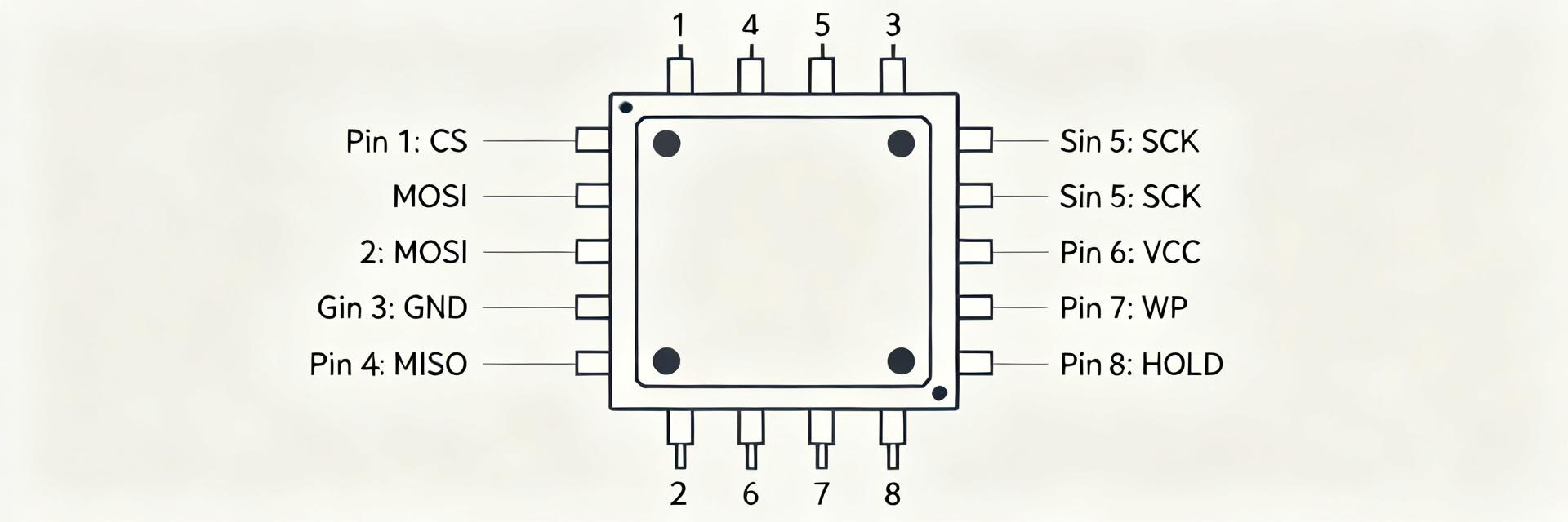
| Serial Interface | 3-wire Microwire | CS, SK, DI, DO signals |
| Max Clock Rate | 3.0 MHz | VCC = 4.5V to 5.5V typical limits |
| Write Cycle Time (t_wc) | 10.0 ms (max) | Self-timed internal programming |
| Supply Voltage | 1.8V to 5.5V | Wide-voltage operation range |
Timing & throughput (read/write latencies, clock limits)
Point: Maximum clock rates are near 3 MHz, yielding predictable read throughput and bounded write latencies. Evidence: At ~3 MHz, serial reads stream bits at the SCLK rate but effective throughput depends on command overhead and host inter‑byte timing. Explanation: Expect single‑word writes to complete on the order of 10 ms per cycle; repeated small writes multiply latency, so aggregate throughput favors block or buffered writes where possible.
Endurance, data retention & reliability indicators
Point: Endurance is limited by write‑cycle counts; retention is often rated in decades under proper conditions. Evidence: Typical serial EEPROM endurance falls in the tens to hundreds of thousands of cycles with retention claims that span decades, but guarantees differ by device revision. Explanation: Treat endurance as a design constraint for frequently updated fields — log updates, employ checksums and avoid tight write loops to preserve device lifetime.
Real-world benchmarks & test methodology (data-driven)
Practical test setup and measurement checklist
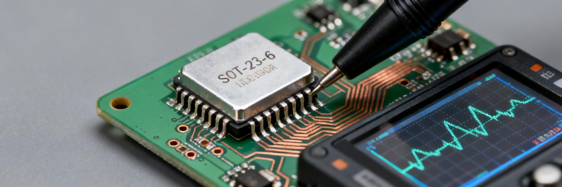
Point: A repeatable bench setup is essential to generate trustworthy metrics. Evidence: Use a controlled VCC supply, level translation where needed, a logic analyzer for command timing and an oscilloscope to capture SCLK and data edges. Explanation: Capture command latency, per‑word write times, active and standby currents, and any bit‑error occurrences; document host timing so results isolate device behavior from controller overhead.
Interpreting benchmark results and performance tradeoffs
Point: Measured times often exceed datasheet numbers due to host overhead and signal integrity margins. Evidence: Host software delays, level shifters and line capacitance reduce effective throughput and can lengthen observed write cycles. Explanation: Balance faster clocks against signal integrity; favor contiguous block writes to amortize command overhead, and consider conservative host timing for reliable transfers in noisy environments.
Typical use cases & implementation examples for 93C46C
Configuration & calibration storage patterns
Point: The 1Kbit capacity suits calibration tables, device IDs and small lookup data. Evidence: Use fixed offsets for records, a version byte, and a CRC or checksum to detect corruption after power events. Explanation: Organize storage with a small header, versioning and a rolling backup record to enable safe firmware upgrades and simple rollback without complex wear leveling for infrequent writes.
Integration examples: MCU interface and power management
Point: MCU firmware must sequence commands carefully and handle power anomalies during writes. Evidence: Implement explicit write polling or status reads, required inter‑command delays and a state machine that blocks critical operations until writes complete. Explanation: Mitigate brown‑out write failures by scheduling noncritical writes, setting a prewrite flag, or caching changes until power is stable and then committing a single atomic write where possible.
Design checklist & best practices (actionable)
PCB, signal integrity and decoupling checklist
Point: Board layout materially affects reliability when clocking near 3 MHz. Evidence: Keep clock and data traces short, control termination, place a 0.1 µF decoupling capacitor close to the device VCC pin and use pull‑ups/pull‑downs on idle lines. Explanation: These measures reduce ringing, lower EMI and prevent spurious toggles; they also reduce the chance of corrupted writes during noisy system events.
Firmware & maintenance best practices
Point: Firmware strategies extend usable life and improve recoverability. Evidence: Batch writes, implement simple wear‑leveling for hot fields, store redundant records and validate with checksums after each write. Explanation: Include production tests — read/write roundtrips, CRC checks and simulated power‑fail during write — to ensure the device behaves within system tolerance before shipping units.
Key summary
- The S-93C46CD0H-T8T2U3 is a compact 1Kbit EEPROM offering 128×8 or 64×16 organization and a 3‑wire serial interface; ideal for small configuration and calibration stores with predictable electrical characteristics.
- Expect maximum clocking near 3 MHz, single‑word write cycles on the order of 10 ms, and endurance/retention that supports decades of data retention under normal use; verify exact numbers for your revision.
- Validate designs with a controlled bench setup capturing command latency, active/standby currents and bit‑error rates; favor batched writes and checksums to protect against power‑fail scenarios and extend lifetime.
Common questions and answers
How does the 93C46C 1Kbit EEPROM compare for small configuration storage?
The 93C46C family is optimized for compact non‑volatile needs: it provides a small footprint, simple 3‑wire Microwire interface and predictable timing characteristics. For configuration or calibration where writes are infrequent, its endurance and retention profile is suitable; designers should use versioning and checksums to protect critical parameters and minimize update frequency.
What performance should I expect when measuring write times and throughput?
Expect single‑word writes to take roughly 10 ms each in typical conditions, with reads limited by the ~3 MHz clock and command overhead. Measured throughput depends on host timing and signal integrity; benchmarking with your controller and layout is necessary to capture realistic end‑to‑end latency and to plan batching strategies.
What are the most important integration checks before production?
Include production tests for read/write roundtrips, CRC verification and power‑fail during a write. Verify PCB decoupling, short signal traces and proper idle pull states. Confirm endurance assumptions by estimating worst‑case update frequency and incorporate wear‑mitigation if critical fields will update often.
How does memory organization and ORG pin configuration affect layout?
The memory organization is dual-mode, offering 128x8 or 64x16 configurations based on the physical state of the ORG pin. Connecting ORG to VCC enables the 16-bit organization, simplifying word-aligned data structures, whereas pulling ORG to GND configures it for byte-oriented 8-bit memory storage.