S-93A86BD0A-K8T2U3: Complete Datasheet Analysis & Key Specs
The S-93A86BD0A-K8T2U3 is a high-reliability 16-Kbit Microwire serial EEPROM housed in a space-efficient 8-TMSOP package. This device is engineered for persistent data storage in environments requiring a low pin-count interface and robust automotive-grade performance.
| Parameter | Specification | Design Impact |
|---|---|---|
| Memory Density | 16 Kbit | Configuration & Calibration Storage |
| Interface | Microwire (3-wire) | Simplified Firmware & Low Pin Count |
| Max Clock Frequency | 2.0 MHz | Standard throughput for small data sets |
| Package | 8-TMSOP | Ultra-compact footprint for dense PCBs |
| Operating Voltage | Wide Range Support | Compatible with 3.3V and 5V Logic |
Quick Product Overview (Background)
Core Function & Capacity
Organized for word/bit efficiency, the S-93A86BD0A-K8T2U3 provides 16 Kbits of non-volatile memory. The Microwire interface (SI/SO/CLK/CS) simplifies PCB routing, making it an ideal choice for storing calibration constants, small logs, and system configuration parameters.
Mechanical & Thermal Grade
The 8-TMSOP footprint is optimized for automotive and industrial systems. Engineers should cross-check the specific temperature grading to ensure thermal suitability for the target environment, while confirming land-pattern dimensions to avoid reflow assembly issues.
Electrical Specs & Performance
Voltage and Timing Parameters
The datasheet specifies a maximum clock frequency of 2 MHz. Critical timing numbers such as tCYC (clock period), tEN (chip-select setup), and tWC (write cycle time) must be extracted to ensure firmware state machines do not violate device boundaries during rapid data bursts.
Power Management
The device features distinct standby, read, and write current profiles. Designers must account for write-cycle peak currents when sizing power-supply decoupling capacitors and budgeting for battery-operated transients.
Reliability & Design Considerations
Endurance & Data Retention
While the device offers high endurance, derating should be applied for high-temperature operations. Implementing wear-leveling or write-caching strategies is recommended for applications with frequent data updates to maximize field service life.
PCB Layout Best Practices
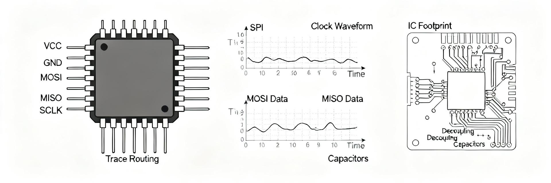
- Place a 0.1 μF ceramic decoupling capacitor as close to the VCC pin as possible.
- Verify the 8-TMSOP land pattern against mechanical drawings to ensure solder joint integrity.
- Add series resistors on signal lines if in-circuit programming (ICP) is required to prevent bus contention.