AT21CS01 1-Wire EEPROM: Protocol & Timing Analysis
Logic-analyzer captures and oscilloscope checks are the fastest way to turn intermittent memory errors into deterministic fixes. Measured waveforms reveal the exact windows where resets, presence pulses and bit samples must occur; applying those measurements to the AT21CS01 removes guesswork from field failures. This guide presents a compact, measurement-led timing analysis for the AT21CS01 1-Wire EEPROM and a reproducible bench procedure engineers can apply during debug and production validation.
Background — Why AT21CS01 and single-wire EEPROMs are used
Device capabilities & electrical interface
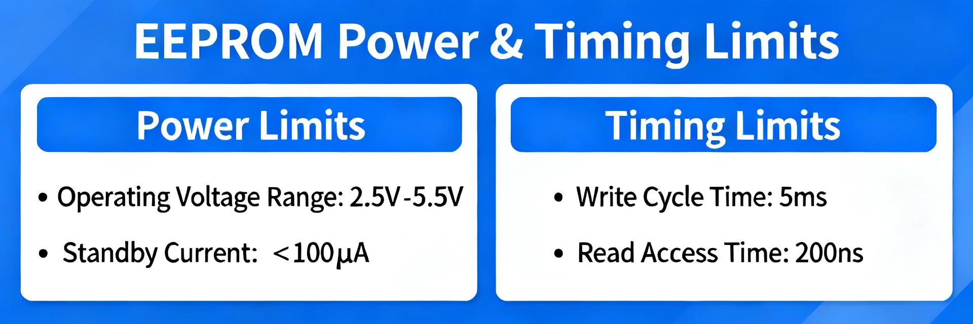
The AT21CS01 provides 1 Kb organized as 128 × 8-bit pages accessed over a single SI/O pin plus ground. The memory map is byte-addressable with page-level write behavior and a single bidirectional data node. This topology constrains bus arbitration, requires careful pull-up sizing and enforces write-cycle timing (endurance typically in the low-to-mid 10^4 cycles), necessitating a budget for write delays and limited endurance.
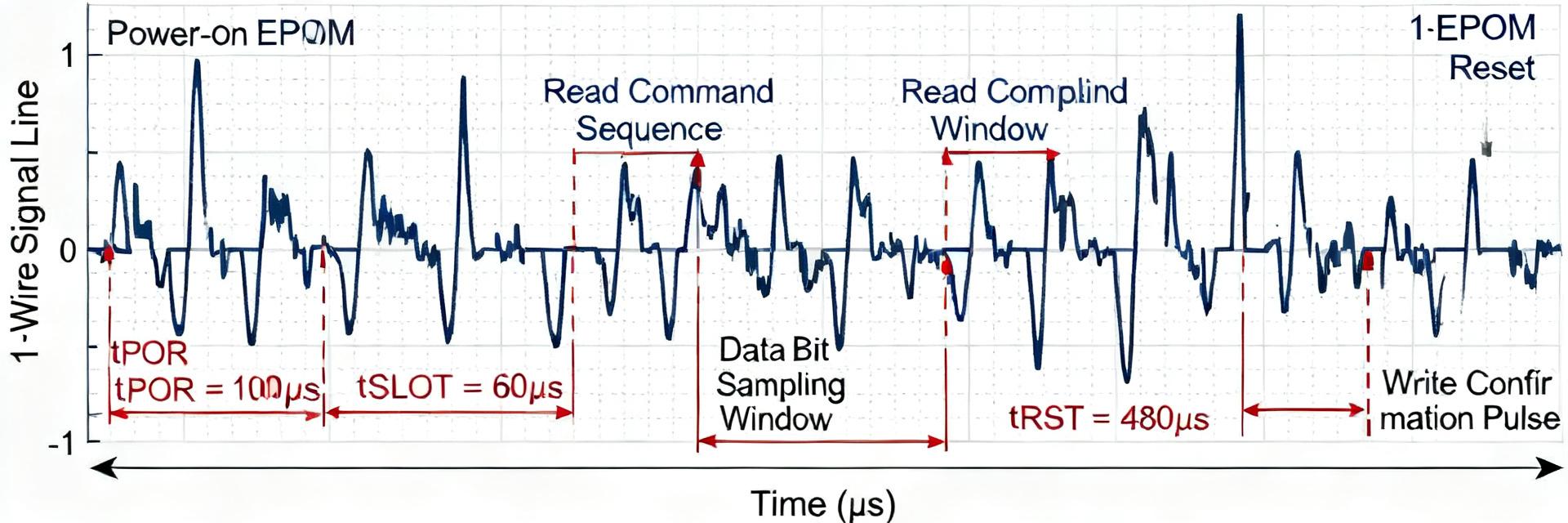
Timing Analysis — Key Parameters
| Parameter | Definition | Suggested Range | Status |
|---|---|---|---|
| tRST | Master reset low time | 200–500 µs | Critical |
| tPRES | Device presence pulse | 60–240 µs | Required |
| tWRITE | Write low duration ('0'/'1') | '0': >50µs, '1': <15µs | Encoding |
| tREAD | Master sample window | 15–30 µs post-release | Stability |
| tREC | Inter-command recovery | ≥1–5 ms | Write Latency |
Implementation Guide — Hardware & Firmware
Hardware Strategies
Choose pull-up values to balance speed and standby current. Resistor choices of 4.7 kΩ–10 kΩ suit short PCB runs; larger harness capacitance benefits from lower values. Lower pull-up reduces rise time but increases current; add series resistors at the master to limit ringing.
Firmware Techniques
Implement calibrated delay loops or hardware-timer-based bit timing. Software loops are sensitive to interrupts; hardware timers provide deterministic windows. Use atomic timing inside critical sections, sample-then-validate reads, and verify writes with a read-back strategy.
/* Pseudo-code: robust read with retries */
for (attempt = 0; attempt < MAX_RETRIES; ++attempt) {
  send_reset();
  if (!detect_presence()) continue;
  send_command(READ_ARRAY);
  for (int i = 0; i < N; ++i) {
    buffer[i] = read_byte_timed(); // Timer-based
  }
  if (validate_crc(buffer)) break;
  delay_ms(backoff_ms(attempt));
}
Summary
- Verify Timing: Measure reset, presence, and bit-write windows under real harness conditions.
- Optimize Pull-ups: Tune resistor values to account for bus capacitance and improve margins.
- Deterministic Sampling: Use hardware timers and read-after-write verification for long-term reliability.
Frequently Asked Questions
How can one reliably measure AT21CS01 presence pulse with a logic analyzer?
Use a falling-edge trigger on the master reset then capture several transaction windows at ≥10 MS/s; measure the device response on the SI/O line looking for a low-going presence after the master releases reset. If the presence is noisy, verify pull-up and probe grounding and re-capture with an oscilloscope at ≥50 MS/s.
What is the recommended approach to debug AT21CS01 read errors over a long harness?
Start by lowering the pull-up incrementally (e.g., from 10 kΩ toward 4.7 kΩ) while monitoring rise time and current; add local ground returns and measure tREAD sample windows. If errors persist, instrument the bus with an oscilloscope to locate ringing or slow edges and switch to hardware-timer sampling.
Which timing parameter most often masks intermittent failures in the field?
tREAD/sample timing is the most frequent culprit because edge slope and sampling offset caused by capacitance or drive strength can flip bits. Ensuring the sample point is centered in the stable portion of the bit window usually eliminates intermittent read errors.
How to ensure internal write completion for AT21CS01?
Enforce a tREC (recovery time) of ≥1-5 ms between the write command and the next access to allow internal non-volatile memory programming. Monitoring the SI/O line for high impedance state can also signal completion in some implementations.