


Helping you save cost and time.

Provide reliable packaging for your goods.

Quick and reliable delivery to save time.

Excellent after-sales service.
New Product Launch
More +


Hot Selling Parts


Blog
S-25C080A0H-T8T2UD Full Datasheet: Pinout, Timing, Specs
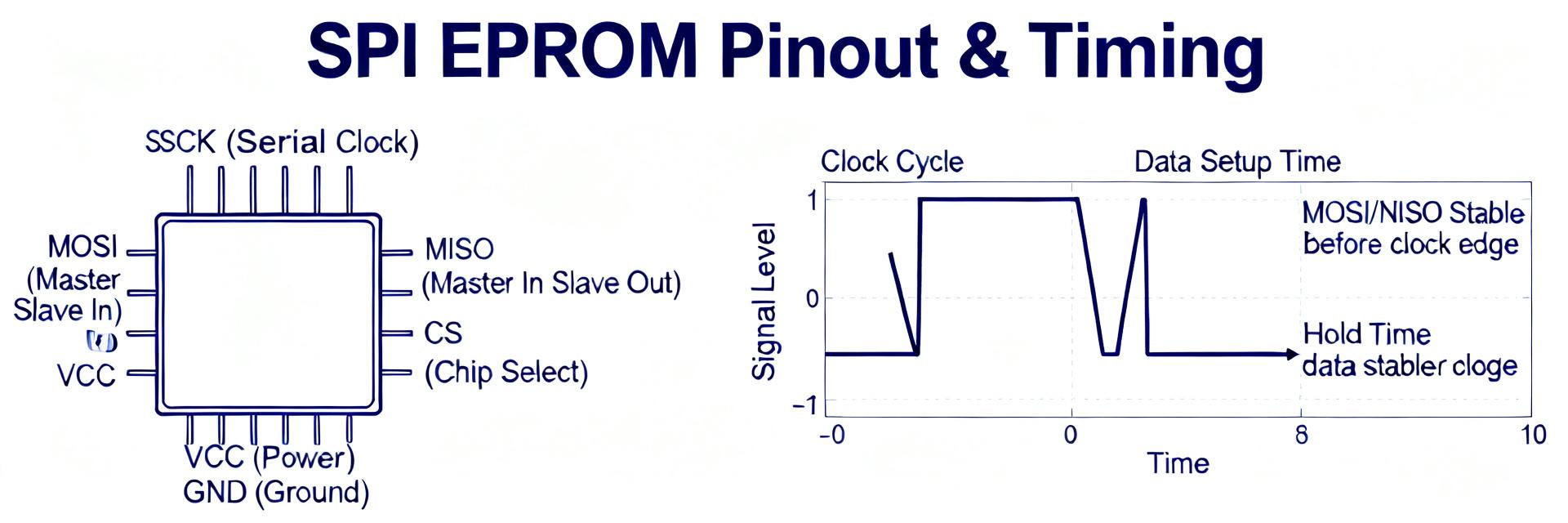
The S-25C080A0H-T8T2UD is an 8-Kbit (1,024-byte) SPI serial EEPROM organized as 1K × 8 bytes (16 blocks × 64 bytes); typical page/block-aware write cycles complete in up to 4 ms and the device support…

S-93A56B EEPROM: Performance Breakdown & Key Specs
Point: This note distills common datasheet benchmarks and lab-test targets for 2K‑bit serial EEPROMs into a concise, actionable profile. Evidence: Typical references for this family show read access t…
S-19190ANH-M6T1U Datasheet: Pinout & Key Specs (Latest)
2026-07-04 10:49:17
S-93C46 Serial EEPROM Data Breakdown: Pinout & Specs
2026-07-03 11:06:10
SPI EEPROM S-25A080B0A-K8T2U3: Key Specs at a Glance
2026-07-02 10:55:11
S-25C320A0H-T8T2U3: Specs & Automotive Reliability Findings
2026-07-01 12:05:10
S-19680 High-Side Switch Performance & Sourcing Analysis
2026-06-29 10:50:12
Read more