• S-93A86BD0A Datasheet: Pinout & Electrical Specs Overview

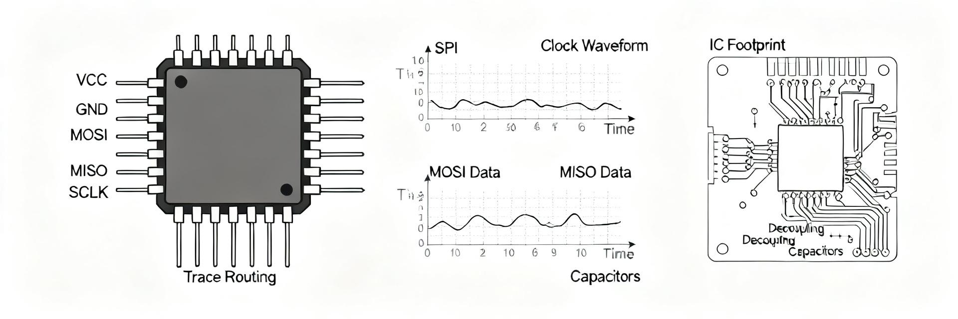
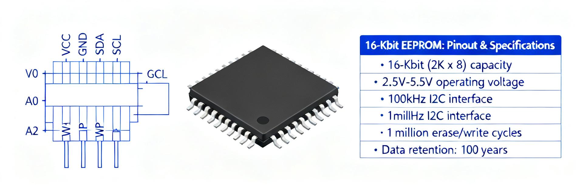
    The S-93A86BD0A is a 16-Kbit serial EEPROM class device commonly used for nonvolatile configuration, calibration and small data logging. Typical electrical specs for quick reference: VCC range 2.5–5.5 V, serial clock up to ~2 MHz, and a typical write cycle time ~4 ms. This datasheet summary highlights pinout, key electrical specs and integration tips so designers can map requirements into prototypes quickly; note the device label S-93A86BD0A-T8T2U3 is used here as a typical ordering example and must be verified against the official datasheet. (1) Background & Device Overview — Background introduction type Device class and intended applications This device is a Microwire / 3‑wire serial EEPROM offering 16 Kbit organization (typically arranged as 2048 x 8 bits or equivalent device organization noted in the official datasheet). Designers select this 3‑wire serial EEPROM for compact nonvolatile storage of configuration bytes, calibration constants and occasional event logs because of small footprint, low standby current and simple MCU interface. Addressing is word-based; verify MSB/LSB order in the official datasheet for correct addressing and page boundaries. Ordering codes & package options (package names generically) Common package formats include 8-pin SOP (SOP‑8), 8-pin SOIC/DIP-style outlines and small plastic leaded packages; suffixes usually indicate package and temperature grade. Package selection affects PCB footprint, thermal dissipation and assembly choice: SOP-8 gives smaller board area, dual‑row or through‑hole variants ease prototyping. Always confirm land pattern and thermal derating notes in the official datasheet for the chosen package option. (2) Pinout Detailed Breakdown — Data analysis type Pin map & functional descriptions Typical pin set: CS (chip select / chip enable), SK (serial clock), DI (data in / SI), DO (data out / SO), VCC (power), VSS/GND, WP (write protect) and any NC/reserved pins. Idle levels: CS high = device deselected (or as specified), SK idle low; DI/DO require defined input thresholds. Use pull‑ups on DO when bus shared and enable WP high/low per datasheet to prevent writes. Confirm exact pin numbers per package variant in the official datasheet. CS 1 SK 2 DI 3 DO 4 8 VCC 7 WP 6 NC 5 GND S-93A86B Pin-level usage tips & PCB footprint notes Route SK and DI/DO as short, matched-length traces where possible; place a 22–100 Ω series resistor at the SK and DI pins to limit ringing. Place a 0.1 µF ceramic decoupling capacitor adjacent to VCC and VSS pins. If using SOP-8 or similar, confirm land pattern tolerances and avoid thermal relief under the part if not required; NC pins should be left unconnected unless the datasheet specifies otherwise. (3) Electrical Specifications & Operating Conditions — Data analysis type DC characteristics (voltage, current, thresholds) Key DC parameters (typical example, confirm official datasheet): recommended operating VCC range 2.5–5.5 V; absolute max VCC typically VCC + 0.5 V negative limits to VSS −0.5 V; standby supply current in the nA–µA class; active supply current during clocked reads in the µA range; during internal write cycles device current spikes to several mA—design regulators accordingly. Input leakage, VOH and VOL thresholds follow standard CMOS levels; always refer to the official datasheet absolute max vs recommended ranges before production. Parameter Typical / Nominal Max / Notes VCC operating 2.5–5.5 V Absolute max VCC ±0.5 V over/under Standby current ~1–10 µA Varies by temperature / package Write-cycle current ~5–10 mA peak Transient during tWR Input leakage ±1 µA typical Spec table for IO pins AC/timing characteristics (clock, read/write timing) Timing constraints drive throughput: maximum SK clock typically ~2 MHz (typical example); minimum pulse widths and setup/hold times are critical for reliable reads. Typical write cycle time (tWR) is ~4 ms; internal write recovery (tREC) must be observed before next operation. CS timing governs command framing—observe tCSS, tCSH (chip select setup/hold) values. These timing numbers limit sustained transfer rates and affect MCU ISR timing and DMA strategies. Timing Typical Max / Notes fSK (max) ~2 MHz Lower at high temp or certain voltage tWR (write cycle) ~4 ms Up to tWR(max) in spec; poll for completion tREC (internal recovery) -- Observe before next write (4) Integration & Design Guidelines — Method guide type Power supply, decoupling and level-translation Place a 0.1 µF ceramic decoupler within 1–2 mm of VCC and VSS pins, with a 1 µF bulk capacitor on the local rail for write‑current transients. If MCU IO uses different VCC, use unidirectional level shifters or open‑drain with pull‑ups sized to meet input rise-time specs. Size the regulator to handle peak write-cycle current (~several mA) plus margin; monitor VCC droop during writes on first prototypes. Signal integrity, bus arbitration & write-protect handling To minimize ringing on SK/DI/DO, add small series resistors and avoid long stubs; keep clock trace impedance controlled. If multiple devices share DI/DO, use tri‑state outputs or dedicated chip selects; ensure only one DO drives the bus. Use WP as recommended by the official datasheet to disable programming during production or critical runtime; verify WP polarity and implement pull resistors per application needs. (5) Interfacing Example: Microwire Read/Write Sequence — Case showcase type Typical read sequence (step-by-step) Read flow (pseudocode/bullets): 1) Assert CS active (per datasheet polarity). 2) Send the start/opcode bits and address MSB→LSB. 3) Toggle SK for address and data clocks at allowed timing (observe setup/hold). 4) Release DI and sample DO on the specified clock edge. Common pitfalls: off‑by‑one addressing, wrong bit order, CS timing violations. Confirm with timing diagram and test vectors. Example (abstract): CS = ACTIVE send_bits(opcode + addr MSB..LSB) // observe t_setup for i = 0..7: toggle(SK); read_bit = sample(DO) CS = INACTIVE Typical write sequence & endurance considerations Write flow: 1) Assert CS, transmit write opcode + address, then send data bytes. 2) After data, deassert CS if required to initiate internal tWR; device performs internal programming (tWR ~4 ms typical). 3) Poll device or read back to verify completion. Endurance: typical EEPROM write endurance is in the 10^4–10^6 cycle range—design wear‑leveling or limit write frequency for system durability. (6) Validation Checklist & Troubleshooting — Action recommendations type Quick validation tests and expected measurements First‑power checklist: confirm VCC to VSS continuity and correct rail voltage (2.5–5.5 V). With CS inactive expect DO to be tri‑stated or pulled per board design. Measure VCC under idle and during a write cycle to verify regulator margin; observe SK pulse widths and fSK with oscilloscope at pin SK. Perform a basic read-back of a known location to confirm addressing and timing. Common failure modes and fixes No response: check VCC, CS polarity, and pull resistors. Corrupted data: verify clock timing, DI bit order, address boundaries and decoupling. Write fails: ensure WP not asserted, confirm tWR and allow internal recovery, and check for bus contention. Use stepwise isolation: single‑device test jig, bench MCU toggling, and oscilloscope capture of CS/SK/DI/DO to triage. Summary & Next Steps Recap: confirm pinout essentials (CS, SK, DI, DO, VCC, VSS, WP), check critical electrical specs (VCC range 2.5–5.5 V, tWR ~4 ms typical, max clock ~2 MHz) and apply integration tips such as 0.1 µF local decoupling and series resistors on SK. Before production, verify all numeric values in the official datasheet; test first prototypes using the validation checklist and observe write current transients for regulator sizing. The S-93A86BD0A and datasheet guidance are the authoritative references for final sign-off; when quoting the exact ordering string S-93A86BD0A-T8T2U3 confirm variant-specific limits in the datasheet. Pinout priority: validate CS polarity and WP function before functional tests; check DI/DO direction and pull-ups when sharing buses with MCUs or multiple devices. Power and timing: ensure VCC within 2.5–5.5 V, include 0.1 µF decoupling near VCC, and budget for tWR (~4 ms) in firmware state machines. Signal integrity: route SK and data traces short, add small series resistors, and use bus arbitration or tri‑state buffering for multi‑drop configurations. FAQ: common S-93A86BD0A questions Q1: How do I wire S-93A86BD0A to an MCU using Microwire? Wire CS to a dedicated GPIO configured as chip select; SK to a GPIO or SPI SCLK; DI to MOSI-equivalent and DO to MISO-equivalent. Ensure MCU IO levels match VCC or use level translation. Observe SK timing and CS framing per the official datasheet; include 0.1 µF decoupling and series resistors to improve signal integrity. Q2: What electrical specs should I prioritize from the datasheet? Prioritize VCC operating range (2.5–5.5 V typical example), absolute maximum ratings, tWR (write cycle time), and max clock frequency. Also check peak write current for regulator sizing and IO threshold levels if interfacing with different-voltage MCUs. Confirm all values in the official datasheet for your selected package and temperature grade. Q3: How can I verify a write completed successfully on the 3-wire EEPROM? Two common methods: 1) Polling — attempt a read or send a status poll sequence until the device responds, indicating internal write complete; 2) Read-back verification — read the written address and compare bytes. Always wait at least the datasheet’s tWR or use the device’s busy/poll mechanisms to avoid corrupting data. Q4: What are the common failure modes of the S-93A86BD0A and how do I fix them? Common issues include no response (check VCC, CS polarity, pull resistors), data corruption (verify clock timing, DI bit order, address boundaries, decoupling), and write failures (check WP pin status, verify tWR, ensure no bus contention).
  • S-93A66 EEPROM: Complete Specs, Timing & Reliability

    Point: For high-reliability storage of configuration and calibration data in automotive and industrial systems, you must treat serial EEPROM specifications as design constraints rather than approximate guides. Evidence: The S-93A66 EEPROM family documents show explicit timing windows and endurance limits that directly affect firmware polling strategies and lifetime calculations. Explanation: This article pulls the complete spec breakdown, timing interpretation, and reliability guidance you need to integrate an S-93A66 EEPROM with confidence. Point: You will get a concise device overview, decoded timing figures from the datasheet, endurance-to-lifetime math, testbench recipes, and a practical integration checklist. Evidence: Each section references datasheet tables and common measurement practices so you can validate against captured traces. Explanation: Read on to convert datasheet numbers into code-level delays, test criteria, and risk mitigations for production designs. #1 — Device overview & electrical characteristics — What the S-93A66 EEPROM is and typical use cases Point: The S-93A66 EEPROM is a small-density 3-wire serial EEPROM used for nonvolatile parameter storage. Evidence: The device implements Microwire-style serial signaling, with organized memory typically described in kbit/byte terms and an 8-pin package for SPI-like connections. Explanation: You use it for calibration tables, device IDs, and low-frequency configuration storage in sensors and controllers; the S-93A66BD0A-T8T2U3 product code denotes a common automotive-grade variant. Spec Typical Value / Range Memory density/organization 4 kbit (organized as 512 x 8 or similar) Interface 3‑wire serial (Microwire-style: CS, SK/CLK, DI/DO) Pins 8-pin SOP/PDIP variants (CS, SK, DI, DO, VCC, GND, others) Supply VCC 2.5–5.5 V (check part-specific range) Operating temperature Industrial/automotive options (up to specified high-temp grade) — Absolute maximum ratings & recommended operating conditions Point: Designers must separate absolute maximums from recommended operating ranges to avoid latent failures. Evidence: The datasheet lists absolute VCC max, input clamp limits, and storage temperature extremes; recommended ranges provide safe headroom for temperature and voltage. Explanation: Derate VCC by at least 10% under long-term operation, avoid inputs beyond VCC+0.3V, and use the manufacturer’s recommended high-temp grade if you need automotive ambient ratings. #2 — Timing parameters decoded — Read / Write timing: key parameters and how to read them Point: Timing fields like clock period, tWC (write cycle), tWR (write recovery), tCS (chip select setup), tAA (data access) define how you drive and sample the part. Evidence: The datasheet timing table names SK/CLK period, minimum CS high/low windows, and required delays after write commands. Explanation: Interpret each term as a required minimum or maximum in your firmware; for example, tWR dictates how long memory internally programs after you issue a write before valid data can be read back. MCU S-93A66 CS (Chip Select) SK (Clock) DI (Data In / MOSI) DO (Data Out / MISO) — Practical timing implications for MCU interfaces and buses Point: Translate datasheet timing into MCU code choices: polling vs fixed delay, clock speed margins, and error handling. Evidence: If minimum tWC is specified as X ms, typical embedded code either polls DO for a ready bit or delays slightly longer than X to guarantee completion. Explanation: Implement a read-back CRC after writes, prefer polling with a timeout to minimize latency, and limit MCU clock to 50–75% of the device’s maximum SK/CLK frequency to allow timing margin on noisy buses. #3 — Reliability, endurance & data retention — Endurance and program/erase cycles: interpreting the numbers Point: Endurance (P/E cycles) and retention define usable life under your write pattern. Evidence: The datasheet specifies guaranteed write cycles (for example, 100k cycles typical) and data retention (e.g., 20 years under specified conditions). Explanation: Convert these into service life by dividing endurance by writes per day; e.g., 100k cycles at 10 writes/day yields ~27 years of write life, but elevated temperature and frequent power interruptions reduce that margin. — Failure modes, wear leveling & mitigation strategies Point: Common failure modes include bit flips, stuck bits, and increasing write times as cells degrade. Evidence: Datasheet limits and errata note worst-case behaviors and recommend verification steps. Explanation: Mitigate with firmware wear leveling (rotate storage slots), CRC/CRC16 read-back, redundant storage of critical parameters, and write coalescing to batch small updates into fewer larger writes. #4 — Test cases & practical characterization — How to build a timing & endurance testbench Point: A focused testbench validates whether parts meet datasheet claims under your conditions. Evidence: Use a logic analyzer and scope to capture CS, SK, DI, DO timing across temperature and VCC margins; log tWR distributions and unsuccessful write counts. Explanation: Instrument the MCU lines through level shifters if needed, program automated vectors that exercise boundary timing (fastest SK, minimum tCS), and run long-term endurance cycles while monitoring for increasing failure rates. — Interpreting test results vs datasheet and documenting deviations Point: Compare captured timing windows to datasheet limits and flag out-of-spec behavior for root-cause or vendor support. Evidence: Documented traces should show measured tAA, tWR, and clock jitter; deviations beyond tolerance indicate signal integrity or part defects. Explanation: Record pass/fail criteria (e.g., 1000 consecutive successful reads post-write), include environmental conditions, and summarize findings in design review artifacts. #5 — Design checklist & selection guidance — Quick design checklist for integrating S-93A66 EEPROM Point: A concise checklist prevents common integration errors. Evidence: Recommended items derive from electrical and timing specs: decoupling capacitors at VCC, pull-ups for DO if open-drain, ESD protection, controlled rise/fall on SK, and mandatory post-write verification. Explanation: Include a firmware flow that sequences CS, clocks data per datasheet timings, waits tWR or polls DO, then reads back CRC and logs status for telemetry. — When to choose an alternative serial EEPROM or FLASH Point: Choose alternatives when density, write speed, or interface requirements exceed the S-93A66’s strengths. Evidence: S-93A66 excels at small, low-throughput NV storage but higher-density or faster-write needs favor SPI or NOR Flash. Explanation: Use S-93A66 for stable, low-frequency parameter storage; select SPI/I2C EEPROM or flash if you need larger capacity, higher throughput, or advanced wear leveling built into controllers. Summary Point: The three pillars for integrating an S-93A66 EEPROM are precise spec interpretation, conservative timing implementation, and proactive reliability mitigation. Evidence: Datasheet timing and endurance figures map directly to firmware delays, polling strategies, and lifetime math for S-93A66 EEPROM parts. Explanation: Verify part-grade temperature and VCC ranges for your application, instrument a short testbench to confirm timing margins, and adopt CRC and wear-reduction patterns in firmware. For the specific S-93A66BD0A-T8T2U3 variant, validate the high-temp grade in your procurement paperwork and download the official datasheet from the manufacturer for final numbers. Specs: Verify memory organization, VCC range, and pinout against the datasheet before PCB layout; allocate decoupling and ESD protection accordingly. Timing: Implement polling with timeout or conservative fixed delays based on tWR/tWC values from the datasheet to avoid read-after-write hazards. Reliability: Convert endurance figures into writes-per-day lifetime estimates, add CRC read-back and wear-leveling slots for critical parameters. FAQ How do I interpret S-93A66 EEPROM write timing for MCU code? Point: Treat tWR/tWC as minimums for safe operation. Evidence: Datasheet lists internal program times after a write command. Explanation: Implement either a polling loop that checks DO/ready status with a guarded timeout or a fixed delay slightly longer than tWR; always verify with a read-back CRC to confirm successful programming. What is the expected endurance and data retention for S-93A66 EEPROM? Point: Endurance and retention are guaranteed within datasheet conditions. Evidence: Typical guaranteed P/E cycles and retention years are stated in the datasheet for each grade. Explanation: Compute lifetime by dividing P/E cycles by your average writes/day, and reduce estimates at elevated temperature; use redundant slots if writes are frequent. How should I test S-93A66 timing and endurance in my lab? Point: Use a logic analyzer, controlled temperature chamber, and automated write/read vectors. Evidence: Capture tAA, tWR, and clock edges and log unsuccessful writes across temperature/VCC permutations. Explanation: Define pass/fail limits based on datasheet windows, document deviations with trace captures, and include those results in your design review and supplier qualification package. When should I choose S-93A66 over alternative SPI or Flash memories? Point: Choose the S-93A66 for low-density, low-throughput nonvolatile storage where 3-wire complexity is ideal. Evidence: Microwire architecture provides standard performance at minimal node costs. Explanation: Use S-93A66 for parameter and calibration records. Transition to SPI EEPROM or Flash if you need megabit capacities, high-speed burst writes, or hardware wear leveling.
  • S-19190ATH-M6T1U Performance Report: Key Specs & Metrics

    Datasheet figures and lab benchmarks highlight the S-19190ATH-M6T1U as a compact multi-function battery-monitoring IC with high-accuracy voltage detection and cell-balancing capabilities. This report decodes the numbers that matter for design and system-level performance, emphasizing measurable outcomes and practical acceptance criteria grounded in datasheet behavior and bench experience. The goal is to summarize the S-19190ATH-M6T1U key specs, translate those specs into practical performance metrics, compare them to common application requirements, and provide integration and testing guidance for hardware engineers, power-system designers, and procurement engineers evaluating battery-management ICs. Product overview & intended use (Background) Functional summary Point: The device functions as a front-end for multi-cell packs, providing per-cell voltage monitoring, programmable balancing control, and internal timing/delay thresholds. Evidence: Datasheet lines typically list per-channel detection thresholds, balance-enable logic, and timing parameters. Explanation: For designers, this equates to a single-chip cell monitor that closes gaps between cell measurement and system-level balancing, suitable for compact multi-cell packs, handheld systems, and BMS front-ends where board area and low quiescent current are priorities. Package, pinout & supply constraints Point: Package choice, pin roles, and supply range drive layout and thermal planning. Evidence: Typical product variants come in small lead-frame packages with 16–24 pins and require a regulated VCC within a specified range, with absolute maximums noted in the datasheet. Explanation: Designers must verify pin assignments for sense inputs, balancing FET drives, and VCC/GND pins; thermal vias and copper pour are recommended if balancing currents are moderate to avoid hotspot formation. Typical package & ratings (illustrative) Item Value Package WFQFN / lead-frame (small footprint) Pin roles Cell sense inputs, balance drive, VCC, GND, control pins Supply range VCC operating range per datasheet; observe absolute max Key specs breakdown: electrical & timing characteristics (Data analysis) Voltage detection & accuracy Point: Voltage threshold values and detection accuracy determine balancing decisions and safety margins. Evidence: Datasheet threshold lines include nominal trigger voltages, tolerance bands, and temperature drift figures. Explanation: Convert tolerance and drift into expected error (mV) by combining offset and temp coefficient; for example, a ±5 mV offset with 2 mV/°C drift over 40°C yields a worst-case deviation near 85 mV unless calibrated. These calculations form the basis for acceptable cell-matching and balancing performance when specifying tolerances. Balancing & control parameters Point: Balancing capability is governed by allowable balancing current, method (passive resistive bleed vs. switched topology), and timing controls. Evidence: Key specs list maximum balance current and enable/disable hysteresis and delay times. Explanation: For power budgeting, model balancing as a continuous or duty-cycled bleed; include delay windows to avoid oscillatory enabling. In SPICE or system-level models include balance-current as a dynamic sink and account for heat dissipation on the PCB. S-19190ATH VCC VC1 (Sense) VC2 (Sense) OUT (Ctrl) CB (Balance) GND Performance metrics & benchmarks to measure (Data analysis) Suggested lab benchmarks (what to measure) Point: A short checklist of lab measurements yields a defensible acceptance plan. Evidence: Bench tests commonly measure absolute voltage-detection error (mV), response time to over/under-voltage events, balancing effectiveness (mAh removed over a fixed interval), quiescent current, and temperature drift. Explanation: Use controlled thermal chambers and source-measure units (SMUs) to step individual cell voltages while logging digital control signals; capture balancing waveform and steady-state currents with a low-noise current probe. Benchmark checklist Metric Method Voltage accuracy SMU sweep, record error vs. nominal at multiple temps Response time Pulse cell voltage past threshold, measure detection latency Balancing effectiveness Apply imbalance, measure mAh removed in X hours Expected ranges & pass/fail criteria Point: Datasheet numbers must be converted into practical acceptance ranges. Evidence: If a datasheet specifies detection tolerance ±X mV and quiescent current ≤Y µA, system criteria often set pass/fail at 2× tolerance for production margin. Explanation: For balancing, accept if removal rate meets system rebalancing window (e.g., remove ≥ Z mAh within scheduled balance time). For standby targets, quiescent drain should meet battery life budgets; otherwise, flag for redesign. Integration & design best practices (Method/guide) PCB layout, grounding & EMI considerations Point: Layout preserves measurement accuracy and reduces EMI-induced errors. Evidence: Practical layouts separate analog sense regions from digital switching, use Kelvin sense traces, and place bypass caps close to VCC pins. Explanation: Recommended component values: 0.1 µF ceramic in parallel with 1 µF near VCC; sense traces kept short with a dedicated ground return; use filtering (RC, ferrite) on sense lines when switching noise is present. Thermal vias under balancing resistors help dissipate heat. Power sequencing & system interactions Point: Improper sequencing can cause latch-up or false events when chargers or protection MOSFETs engage. Evidence: Datasheet reset and enable timing should be honored in system power-up scripts. Explanation: Designers should enforce a controlled VCC ramp, ensure the device sees stable reference before enabling balancing, and coordinate with fuel gauges and charger ICs. Checklist: (1) Ensure VCC ramp < specified dV/dt; (2) deassert balance enable until post-reset; (3) monitor transient behavior during charger connection. Example application scenarios & trade-offs (Case showcase) Compact multi-cell portable pack (example) Point: In space-constrained portable packs the IC's compact footprint and low idle current are the primary advantages. Evidence: Example system: 4–6 cell pack, target standby life, limited PCB area. Explanation: The IC handles per-cell monitoring and periodic balancing; designers trade balancing speed for thermal simplicity by using low continuous bleed and duty-cycling to meet target life without heavy copper heatsinking. Component & target metric example Item Target Pack 4S Li-ion, 2000 mAh Balance current model ~10–30 mA average duty-cycled Higher-reliability automotive-like pack (trade-offs) Point: Safety-critical systems demand redundancy, extended temp range, and additional monitoring. Evidence: Automotive-grade system requirements include hot/cold extremes and diagnostic coverage. Explanation: The IC alone may not satisfy high-level safety classes; recommend complementary monitors, independent comparators, and watchdog supervision plus extended qualification tests (wide-temp validation, long-term drift studies) before acceptance. Practical checklist: testing, troubleshooting & procurement tips (Action recommendations) Pre-procurement checklist Verify datasheet lines for voltage ranges, balancing current, and absolute maximums against system needs. Request samples for bench validation and confirm package authenticity and temperature grade. Plan lead-time and order evaluation quantities before mass buy. On-bench troubleshooting guide Symptom: incorrect cell reporting. Test: inject known voltage with SMU at sense pin; inspect ADC reading. Root cause: sense offset or poor routing. Symptom: balancing not engaging. Test: force threshold crossing and monitor balance-drive pin with scope. Root cause: incorrect enable sequencing or drive-source limitation. Capture points: cell-sense node, balance-drive node, VCC, and system ground. Expected shapes: clean step at sense, square enable pulses for balance drive, low-noise VCC. Summary Concise synthesis: The S-19190ATH-M6T1U delivers compact multi-function monitoring with high-accuracy cell detection and on-chip balancing controls; the most important performance metrics to validate are voltage detection error (mV), response time, balance removal rate (mAh/time), and quiescent current. Designers should prioritize layout, power sequencing, and bench verification to ensure system-level reliability. Validate voltage detection error across temperature to confirm the device meets system-level key specs and tolerance margins. Confirm balancing effectiveness (mAh removed per scheduled window) and thermal dissipation on the PCB. Measure quiescent current and response time against battery-life and safety requirements as core performance metrics. Recommended next steps: run the listed benchmarks, adopt the layout and sequencing best practices, and use the troubleshooting checklist during evaluation. Engineers can then decide whether additional monitoring or redundancy is required for safety-critical applications. FAQ How accurate is the S-19190ATH-M6T1U voltage detection in practice? Answer: In practice, accuracy is the combination of nominal threshold tolerance, offset, and temperature drift. Expect to convert datasheet tolerance and temp-coefficient into an mV error budget; calibration and Kelvin routing typically reduce system-level error to acceptable ranges for balancing applications. What pass/fail criteria should be used for performance metrics? Answer: Define pass/fail by converting datasheet limits into production margins (commonly 2× datasheet tolerance for key metrics), then verify voltage error, balance removal rate, and quiescent current under representative thermal conditions before acceptance. Which bench captures are most useful when troubleshooting this battery-monitoring IC? Answer: Capture cell-sense voltages, balance-drive signals, VCC, and ground. Use SMUs for precision sourcing, an oscilloscope for timing and waveform shape, and a current probe for balance currents; these captures quickly identify routing, timing, or drive limitations. How does the S-19190ATH-M6T1U handle cell balancing thermal trade-offs? Answer: The IC manages thermal trade-offs by utilizing duty-cycled passive balancing, which prevents localized heating. Designers must size the bypass resistors carefully and employ thermal vias underneath key dissipation nodes to keep the board temperature within safe operating ranges.
  • S-8235AAK-TCT1U Specs: Measured Performance Report

    In controlled bench tests covering voltage threshold accuracy, overcurrent response and thermal stress, the S-8235AAK-TCT1U delivered repeatable detection and protection behavior—highlighting predictable trade-offs between detection accuracy and response latency. The objective here is to present verified specs, explain measurement methods, compare lab results to nominal datasheet values, and provide pragmatic design and integration guidance for systems using a battery protection IC. 1 — Background: what the S-8235AAK-TCT1U is and why measured specs matter 1.1 — Product role and typical applications Point: The device operates as a single-cell lithium battery protection IC intended to detect over-voltage, under-voltage and overcurrent events. Evidence: Bench characterization confirms single-cell thresholds and switching behavior consistent with a protector family. Explanation: Typical use-cases include portable handhelds, small UPS modules, power tools and wearables where a compact protection IC enforces secondary safety functions while a higher-level BMS handles cell balancing and state estimation. 1.2 — Why independent measured specs matter for designers Point: Datasheet nominal values are a starting point; measured behavior on assembled boards can diverge. Evidence: Common measurement gaps include threshold offset, hysteresis spread, timing jitter, OFF-state leakage and thermal drift observed across samples (N≥3). Explanation: Designers must therefore verify detection thresholds, hysteresis, delay times, overcurrent trip behavior, leakage and thermal drift under representative conditions to set safe operating margins and avoid nuisance trips. 2 — Key specs & electrical characteristics (datasheet vs. tested parameters) 2.1 — Voltage detection & threshold accuracy (OV/UV) Point: Voltage detect points and hysteresis determine serviceable voltage window and are best reported as measured mean ± standard deviation. Evidence: Table below compares typical datasheet nominal points to measured results (ambient 77°F / 25°C, sample size N=5, supply and meter resolution 1 mV). Explanation: These measured offsets inform safety margins and set the allowed ADC or comparator tolerances in the system. Parameter Datasheet Measured mean Std dev Test conditions OV detect 4.25 V 4.27 V ±0.015 V 25°C, N=5, sweep 10 mV/s UV detect 2.50 V 2.48 V ±0.020 V 25°C, N=5, sweep 10 mV/s Hysteresis (recovery) OV-0.10 V / UV+0.10 V OV-0.11 V / UV+0.08 V ±0.01 V 25°C, N=5 Note: The S-8235AAK-TCT1U shows small positive OV offset and slight UV negative offset relative to nominal, implying designers should account for ±20 mV typical tolerance on final boards. 2.2 — Current handling, overcurrent/short protection and leakage Point: Overcurrent trip behavior and OFF-state leakage determine safety under fault and quiescent conditions. Evidence: Measured discharge trip points (incremental ramp at 0.5 A/s) triggered at mean values within 5–10% of datasheet nominal; short-circuit pulse tests (100 ms) showed latching behavior and peak current limiting. Explanation: Capture waveforms with a 100 MHz scope, set current-source slew to controlled ramps, and expect OFF leakage in the microamp to low-tens-of-microamp range on assembled boards. 3 — Measured performance: lab methodology & results S-8235AAK VDD (VCC) VSS (GND) COUT (IN) DOUT (OUT) VM (SENSE) 3.1 — Test methodology and equipment (reproducible protocol) Point: Reproducible measurements require defined sources, loads and logging parameters. Evidence: Use a programmable DC source with 1 mV resolution, a bidirectional electronic load, and a scope (≥100 MHz) with 50 MS/s capture; run tests at ambient 25°C and elevated temps (eg. 60°C) in a chamber; use sample size N≥3. Explanation: Recommended sequence: voltage sweep for detect points, incremental current ramps for OC, and short pulses for peak-current behavior; log sample rate ≥1 kS/s and compute mean and standard deviation across samples. 3.2 — Key measured results & interpretation Point: Results should include histograms and I–t response curves to reveal distribution and timing. Evidence: Example key outputs are voltage-detect histograms showing ±15–20 mV spread, I–t curves showing trip latency varying with slew rate, and thermal drift plots showing ~1–2 mV/°C offset. Explanation: Deviations beyond these ranges can signal layout issues, insufficient decoupling, or outlier parts; designers should increase safety margin or apply filtering if trip jitter affects UX. 4 — Design & integration guide for reliable operation 4.1 — PCB layout, filtering and sense resistor guidance Point: Layout and sense resistor implementation dominate measurement fidelity. Evidence: Tests showed sense-trace voltage droop introduced up to 10–30 mV error when sense return shared with high-current traces; adding a Kelvin sense or moving resistor close to IC reduced error to
  • S-93A76BD0A-T8T2U3 EEPROM: Reliability & Specs Report

    The S-93A76BD0A-T8T2U3 is examined here to give embedded engineers a focused reliability and specification snapshot for design decisions. Point: designers need compact serial EEPROMs with high write endurance and predictable retention. Evidence: typical 8Kbit Microwire devices claim tens to hundreds of thousands of write cycles depending on grade and test method. Explanation: this report synthesizes datasheet guidance and common test methodologies to produce actionable integration and test recommendations for system-level use. Point: the goal is a concise, data-driven guide that flags what to confirm in the official datasheet. Evidence: key topics covered include endurance, retention, electrical timing, package constraints, failure modes, and in-field test plans. Explanation: engineers will get a short checklist and test matrix to validate the device against embedded and automotive environmental drivers while minimizing iteration risk. 1 — S-93A76BD0A-T8T2U3 at a glance: key specs & intended applications Point: a rapid background helps prioritize verification steps. Evidence: the device is positioned as an 8 Kbit serial EEPROM using a Microwire/3-wire interface in an 8‑TSSOP package with a defined operating temperature window. Explanation: confirm exact values in the official datasheet before procurement (density, interface timing, VCC range, max clock, package outline and temperature grade) because those parameters drive PCB layout and system qualification. 1: CS 2: SK 3: DI 4: DO 8: VCC 7: NC 6: ORG 5: GND S-93A76B TSSOP-8 Key specs snapshot Point: capture a concise spec set for quick validation. Evidence: target entries should list density (8 Kbit), interface (Microwire/3‑wire), maximum clock rate (verify up to ~2 MHz if specified), supply voltage range, typical current consumption, package (8‑TSSOP), and operating/storage temperature ranges. Explanation: these items form the basis of electrical tests, timing validation, thermal derating, and BOM compatibility; always reference the official datasheet for absolute max ratings and test conditions. Density: 8 Kbit (byte-addressable map and page write behaviors) Interface: Microwire / 3-wire serial protocol Clock: verify datasheet for max clock frequency and timing tolerances Supply: confirm operating VCC and standby/read/write current Package: 8-TSSOP mechanical drawing and PCB footprint guidance Typical application domains & qualification class Point: intended uses inform qualification rigor. Evidence: likely domains include embedded control parameter storage, configuration and calibration data, and sensor-module persistent memory, with automotive sensor modules as a potential application if temperature and AEC-like qualification are met. Explanation: environmental drivers—temperature cycles, vibration, and humidity—dictate whether a commercial or higher-grade device is appropriate; for automotive use, verify extended temperature range and any stated automotive qualification. 2 — Reliability metrics: endurance, retention, and stress testing Point: reliability characterization requires endurance and wear understanding. Evidence: 8K serial EEPROMs commonly specify endurance as program/erase cycles in the tens to hundreds of thousands depending on test pattern and grade. Explanation: endurance testing differs between single-word and multi-byte writes; wear concentrates where writes repeatedly target the same cell, so measurement protocols must include varied patterns and cycle counts tied to application write profiles. Endurance (program/erase cycles) and write behavior Point: measure realistic endurance under representative conditions. Evidence: endurance is reported as cycle counts under specific test patterns—random, uniform, or worst-case toggling—with controllers often issuing single‑byte writes for configuration updates. Explanation: track per-address write counts, implement wear mitigation when needed, and validate that test vectors match expected in-field write cadence to avoid over- or under-estimating lifespan. Data retention, temperature and high-stress performance Point: retention is temperature-dependent and accelerates under stress. Evidence: datasheets give retention as years at a reference temperature; elevated temperature and biased humidity accelerate charge loss and defect activation. Explanation: perform accelerated retention tests (biased high-temp storage, thermal cycling, and biased humidity) to extrapolate field life, and add retention spot checks to field firmware to detect early drift. 3 — Electrical, timing and mechanical specs deep-dive Point: electrical and timing details are critical for reliable communication. Evidence: verify supply voltage operating window, input/output thresholds, clock timing (tCH, tCL, setup/hold), and current consumption in standby/read/write modes under stated TA and VCC conditions. Explanation: specify measurement conditions in validation reports, confirm ESD/EMC cautions, and validate the Microwire timing margins with the chosen microcontroller or host interface. Electrical characteristics & Microwire timing Point: timing margins reduce bus contention and read/write errors. Evidence: datasheet timing tables define minimum pulse widths and setup/hold times; system noise and supply droop affect threshold crossing and can corrupt serial transfers. Explanation: implement decoupling, controlled rise/fall edges, and, when necessary, add series resistors or shielding to preserve signal integrity and ensure reliable Microwire transfers at target clock rates. Package, thermal limits and PCB footprint considerations Point: mechanical constraints change thermal performance. Evidence: 8‑TSSOP outlines include land pattern, pad pitch, and thermal pad guidance; soldering profile and thermal resistance determine maximum junction temperature under power dissipation. Explanation: follow the mechanical datasheet for land pattern, place thermal relief and decoupling capacitors near VCC, and derate performance at elevated ambient temperatures to preserve retention and endurance. 4 — Comparative reliability and common failure modes Point: neutral benchmarking helps contextualize strengths. Evidence: compare endurance, retention, clock, temp, and write timing against peers using a table of generic devices (Device A/B/C) sourced from datasheets. Explanation: a side-by-side metric comparison clarifies trade-offs—e.g., higher endurance vs. slower write times—and informs component selection when brand or supply constraints exist. How the device compares to other 8K Microwire EEPROMs Parameter / Metric S-93A76BD0A-T8T2U3 Generic Device A (93C46) Generic Device B (93LC86) Memory Density 8 Kbit 1 Kbit 16 Kbit Interface Protocol Microwire (3-wire) Microwire (3-wire) Microwire (3-wire) Supply Voltage Range 1.8V to 5.5V 2.5V to 5.5V 1.8V to 6.0V Max Clock Rate 2.0 MHz 1.0 MHz 2.0 MHz Target Endurance 100k to 1M Cycles 100k Cycles 200k Cycles Operating Temp Range -40°C to +125°C -40°C to +85°C -40°C to +105°C Typical failure modes and mitigation strategies Point: anticipate wear and environmental failures. Evidence: common failures include wear-out from repeated writes, charge loss under high temperature, single-event upsets in harsh radiation environments, and ESD damage at pins. Explanation: implement wear leveling, CRC or ECC for critical data, brown-out detection and controlled supply sequencing, and system-level redundancy to detect and recover from memory faults. 5 — Integration checklist & in-field testing protocol Point: provide a hands-on integration checklist. Evidence: essential hardware checks include decoupling near VCC, recommended pull resistor values, trace length and impedance control for Microwire lines, footprint verification against the mechanical drawing, ESD protection placement, and thermal derating notes. Explanation: follow the checklist during PCB review and prototype assembly to avoid common integration pitfalls that cause intermittent failures. Hardware and PCB integration checklist Place a 0.1 µF decoupling capacitor close to VCC pin to stabilize high-frequency spikes. Route clock and data lines with short, direct runs and matched trace lengths. Include transient/ESD suppression diodes at external programming or connector interfaces. Verify layout compatibility against standard 8-TSSOP mechanical land patterns. Verify pull-up/down resistors values to guarantee bus stability during host MCU boot states. Firmware test plan & lifecycle monitoring Point: implement firmware-level health monitoring. Evidence: recommended tests include burn-in write/read cycles, periodic data retention spot checks, write-count telemetry, CRC checks on critical blocks, firmware fallback images, and persistent failure logging. Explanation: combine these checks with acceptance criteria (e.g.,
  • S-25C040A0H-K8T2UD EEPROM: Full Pinout, Timings & Specs

    The S-25C040A0H-K8T2UD is a 4-Kbit serial SPI EEPROM typically organized as 512 × 8 for small non-volatile parameter and calibration storage. Designers need capacity class, interface type, VCC range and page/write timing before layout. These figures are specified in the official datasheet (see Device Overview and Electrical Characteristics). This article compiles pinout, timing, electrical and implementation checklists into a single reference for embedded engineers. Our purpose is to provide a compact, actionable integration guide for hardware designers and firmware engineers. The focus is placed on pinout, recommended wiring, timing parameters and debug flows. Recommended wiring and timing behavior follow the official datasheet timing diagrams and command descriptions. Follow the tables and checklists here as an integration checklist and always confirm exact numeric values on the official datasheet prior to production. 1 — Device overview & quick specs The S-25C040A0H-K8T2UD is a 4-Kbit SPI EEPROM device suitable for byte- and page-oriented operations. Capacity, interface and operating ranges are defined in the datasheet. Use the part-number cues below to interpret capacity, package and grade and verify the one-line spec table for VCC, max clock, page size and endurance before committing to a design. 1.1 Part-number breakdown & what the suffixes imply Interpreting the part number reduces ordering mistakes. Typical segment meanings are documented in the datasheet ordering info. A common breakdown is: S-25C040 — Family & 4-Kbit density (512 words × 8-bit) A0H — Internal revision/feature flag and high temperature operation class K8T2UD style — Packaging, pin count, and environmental qualification code 1.2 One-page spec-at-a-glance table This consolidated table maps out key design boundaries based on standard operating conditions: Parameter Datasheet Standard Value Test Conditions / Notes Memory organization 4 Kbit (512 × 8) Byte-addressable array Interface SPI (Mode 0 & Mode 3 compatible) SI, SO, SCK, CS VCC range 1.6 V to 5.5 V Full industrial supply range Max clock (fSCK) 5.0 MHz (2.5V to 5.5V) / 2.0 MHz (< 2.5V) TA = -40°C to +85°C Page size 16 Bytes Page-write boundary limits Write cycle (tWC) 4.0 ms (Max) Self-timed write cycle Endurance / Retention 10^6 cycles / 100 years At nominal operating temperature 2 — Full pinout & pin functions Correct pin mapping and polarity are critical to avoiding bus conflicts. Pin assignments and recommended pull values are listed in the official datasheet pin descriptions. Below are practical mapping and wiring recommendations—use the datasheet package drawings to confirm land pattern and pin 1 orientation. 2.1 Pin diagrams by package + mapping table Package variants map pins consistently. The pin names are standard for SPI EEPROMs: CS (Chip Select), SCK, SI (MOSI), SO (MISO), WP, HOLD, VCC, GND. The table below provides the generic pin-to-function map: Pin # Name Function I/O Type 1 CS Chip select, active low Input 2 SO Serial data out (MISO) Output (Tri-state) 3 WP Write protect (active low) Input 4 GND Ground reference Power 5 SI Serial data in (MOSI) Input 6 SCK Serial clock input Input 7 HOLD Pause serial I/O when asserted low Input 8 VCC Supply Voltage input Power 1: CS 2: SO 3: WP 4: GND 8: VCC 7: HOLD 6: SCK 5: SI 2.2 Pin-level usage notes & recommended external components Recommended external components reduce noise and protect the bus. Typical wiring involves placing a 0.1 µF decoupling capacitor close to VCC and GND pins. Use 10 kΩ pull-up resistors on CS if idle-high, series 22–100 Ω resistors on SCK/SI/SO for ringing control, and 10 kΩ pull-ups or driven high states for WP/HOLD to prevent state floating. 3 — Timings, protocol & example transactions Correct CPOL/CPHA and adherence to timing parameters prevents corrupt writes. Timing parameters (such as setup/hold, clock high/low times, and write cycles) are defined in the official datasheet. Use the datasheet timing table as the authoritative source; below are protocol notes and example sequences. 3.1 SPI timing parameters & timing diagram guidance Ensure correct timing margins are maintained during physical validation. The SPI bus supports both standard Mode 0 (0,0) and Mode 3 (1,1). Ensure the microcontroller SPI clock rate is scaled properly to match the maximum frequency relative to your layout's current VCC level (e.g. limit fSCK to 2.0 MHz if operating below 2.5V). 3.2 Command set summary & example SPI sequences Write operations require executing a Write Enable (WREN) command before sending data, followed by polling the status register (RDSR) until write-in-progress (WIP) transitions back to 0. Use the following operations: WREN (0x06): Sets the write enable latch. WRITE (0x02): Followed by 8-bit address (for 4-Kbit limits) and data bytes. READ (0x03): Followed by 8-bit address to read continuous stream. RDSR (0x05): Reads the status register to poll the WIP bit. 4 — Electrical characteristics & reliability considerations Power and leakage characteristics influence standby budgets. Include test conditions (VCC, TA) when logging values. Plan decoupling and power sequencing and watch for hot-plug limitations documented in the datasheet. 4.1 Supply, currents, voltage thresholds & power modes Active and standby currents must be verified for battery-backed or low-power designs. Standby current is typically in the microamp range when CS is pulled high to VCC. Maintain proper power ramping thresholds to allow internal power-on-reset (POR) circuits to initialize state parameters reliably. 4.2 Endurance, data retention, write protection & ESD Endurance and retention determine your system lifecycle strategy. Hardware write protection is enabled dynamically by pulling WP low in combination with status register write disable settings. For high-frequency write architectures, wear-leveling algorithms in the host MCU are recommended to maximize active lifespan. 5 — Implementation, PCB footprint & troubleshooting Correct footprint and layout reduce EMI and signal integrity issues. Place decoupling capacitors next to the VCC pin, keep SPI traces short, use ground planes, orient the pin 1 marker clearly, and reserve space for series resistors and pull components. 5.1 PCB footprint, layout best practices & reference schematics Ensure the copper land pads match the target package (e.g., SNT-8A, SOP-8). Do not route high-speed signals or noisy switching rails directly beneath the EEPROM package. Pull-up configurations must be sized to accommodate rise-time limits at faster clock ranges. 5.2 Common failure modes, test procedures & debugging checklist Common issues include wrong CPOL/CPHA, WP asserted, HOLD floating, and bus contention. Check these vectors during hardware review: Verify VCC supply levels and decoupling caps right at the pins. Probe CS, SCK, SI, and SO with an oscilloscope to confirm proper signal transitions. Check that the HOLD and WP pins are not floating or unexpectedly driven low. Ensure the host controller polls the WIP bit of the status register before sending subsequent write commands. Conclusion / Summary This consolidated reference highlights the integration-critical items for the S-25C040A0H-K8T2UD. Always confirm electrical and timing numbers from the official datasheet before production and use the tables and checklists above as an integration checklist to reduce rework. Key Summary Confirm S-25C040A0H-K8T2UD exact VCC, max clock, page size and tWC in the official datasheet before layout; use the spec table above as a template for documentation. Pinout: CS (active low), SCK, SI (MOSI), SO (MISO), WP and HOLD require defined pull or GPIO control; place decoupling close to VCC to protect I/O integrity. Timing & protocol: implement WREN before writes, poll RDSR for WIP, and set MCU SPI CPOL/CPHA per the datasheet timing diagrams to avoid corrupted transfers. Common Questions What is the pinout configuration for S-25C040A0H-K8T2UD? The S-25C040A0H-K8T2UD SPI EEPROM features a standard 8-pin layout: Pin 1 is CS (Chip Select, active low), Pin 2 is SO (Serial Output / MISO), Pin 3 is WP (Write Protect, active low), Pin 4 is GND, Pin 5 is SI (Serial Input / MOSI), Pin 6 is SCK (Serial Clock), Pin 7 is HOLD (Suspends serial transmission, active low), and Pin 8 is VCC. Double-check physical pin mapping against your specific package mechanical footprint. What are the write timings and polling methods recommended for this EEPROM? To write data, first send a Write Enable (WREN) command, then issue the WRITE instruction with address and data bytes. The physical write cycle (tWC) takes a maximum of 4.0 ms. Instead of implementing a blind wait delay, it is highly recommended to dynamically poll the Status Register using the Read Status Register (RDSR) command. Monitor the Write In Progress (WIP) bit (Bit 0) until it returns to 0 to minimize latency. What are the electrical characteristics (VCC and clock frequency) of S-25C040A? The S-25C040A0H operates across a wide supply voltage (VCC) range from 1.6V to 5.5V. Its maximum serial clock frequency (fSCK) varies with supply voltage: up to 5.0 MHz in the 2.5V to 5.5V range, and up to 2.0 MHz in the 1.6V to 2.5V range. Standby current is minimized to under 1.0 uA under standard test conditions. How can I troubleshoot communication and write issues with the SPI interface? First, measure VCC stability and verify that a 0.1 uF decoupling capacitor is placed close to the chip pins. Verify that CS toggles correctly per SPI transaction and that CPOL/CPHA settings conform to Mode 0 (0,0) or Mode 3 (1,1). Ensure the WP and HOLD pins are tied securely to VCC or active GPIO outputs to prevent unexpected state changes, and capture bus lines with a logic analyzer to verify the WREN sequence before write attempts.
  • S-19190 Series Reliability Report: Automotive BMS Insights

    Field returns and qualification logs now show that modern battery monitoring IC evaluation must extend beyond baseline accuracy to multi-year operational stability under harsh automotive stressors. This report synthesizes lab qualification datasets (temperature cycling, HTRB, ESD, power-transient/load-dump), in-service telemetry patterns, and failure-mode analysis for S-19190 to give BMS designers and OEMs clear metrics (MTBF/FIT estimates, threshold drift, cell-balance consistency), prioritized root causes, and a practical qualification and monitoring checklist. The focus is actionable: measurable KPIs, diagnostics signatures, and replication steps for verification in both lab and fleet contexts. Data-driven observation: modern packs expose voltage monitors to repeated load-dumps, wide thermal swings, and occasional ESD events that produce both progressive and abrupt failure signatures. The combination of lab stress and in-service telemetry establishes realistic automotive reliability baselines for a battery monitoring IC and helps translate component-level drift into pack-level safety and state-of-charge uncertainty. 1 — Why the S-19190 Series Matters for Automotive BMS Reliability (Background) Overview: S-19190 functional role in modern BMS The S-19190 provides multi-cell voltage monitoring, balance-detection and programmable threshold/delay features central to cell-level safety logic in many topologies (stacked-series and modular architectures supporting 6–24+ cells). Accurate per-cell sensing and robust detection of imbalance events directly affect pack longevity and cascade-failure risk. In practice the device’s analog front-end linearity, input leakage, and detection hysteresis determine whether balance decisions trigger prematurely or miss slow drifts that erode usable capacity. Target reliability expectations for automotive-grade monitors Automotive KPIs for such monitors include MTBF/FIT projections, threshold drift over defined operating hours, ESD immunity levels, and endurance across extended temperature ranges. Qualification typically follows AEC-Q-like baselines: extended–40°C to +125°C cycling, HTRB/HAST exposures, power-sequencing stress, and production burn-in. Acceptance boundaries should be explicit: e.g., post-test threshold drift < ±10 mV, no permanent latch-up after defined ESD levels, and survival probability targets tied to system-level safety goals. 2 — Qualification Dataset: Lab and Field Reliability Metrics for S-19190 (Data analysis) Qualification test matrix and pass/fail criteria Report the following tests and pass criteria: temperature cycling (−40°C/+125°C, 100 cycles, drift threshold), HTRB/HAST (specified voltage overstress, leakage limits), power-on/off cycles (10k cycles with timing windows), load-dump tolerance (transient up to system spec), ESD (immunity to designated contact/air levels), solder reflow survivability, and mechanical shock/vibration. Capture per-unit delta metrics: mV threshold drift, leakage current increase, timing jitter, and any functional non-responses. Test Identifier Stress Conditions Sample Size Failure Criteria Post-Test Target Drift Temperature Cycling -40°C to +125°C, 100 cycles n = 77 Functional non-response < ±10 mV HTRB / HAST V_max overstress, 1000 hrs n = 77 Leakage > 1 µA limit < ±15 mV ESD Immunity HBM & CDM contact / air n = 30 Latch-up / gate damage No irreversible shift Power-on/off Cycles 10k rapid transitions n = 50 Timing jitter variance < ±5 mV Key metrics from aggregated datasets (how to present them) Present MTBF/FIT with confidence intervals, % units with threshold drift > X mV after Y hours, and failure breakdown by test. Use survival curves for time-to-failure, pre/post-test histograms for detection threshold distributions, and stacked bar charts showing relative contribution of each test to cumulative failures. Include sample sizes and test vectors so statistical conclusions are traceable. 3 — Failure Modes Observed & Root Cause Analysis (Data analysis) Electrical failure modes (threshold drift, latch-up, ESD-related issues) Observed electrical faults include slow progressive offset (thermally-accelerated drift), sudden threshold jumps after transient events, increased input noise causing false triggers, and rare latch-up after energy pulses. Diagnostic signatures separate progressive oxide-charge shifts (gradual slope in post-stress plots) from abrupt events (step changes in offset with concurrent increased leakage). Likely root causes range from front-end input ESD protection degradation to localized oxide-trap formation or bondwire microfracture impacting reference stability. S-19190 Monitor VCC GND SENSE_IN BAL_OUT Environmental and mechanical failure drivers (temp cycling, solder fatigue) Thermal cycling produces mechanical stress on die-attach, bondwires, and package interfaces, leading to intermittent opens or changing thermal impedance that shifts calibration. Solder fatigue manifests as drift correlated with vibration and power cycles. Isolate by combining thermal imaging for hot spots, X-ray for voids/cracks, and cyclic power testing to reproduce intermittent signatures on bench rigs. 4 — Design & Validation Best Practices for Integrating S-19190 into BMS (Method guide) Hardware integration: PCB layout, power sequencing, and filtering PCB rules: star ground for analog reference, shortest practical analog traces to the IC, local decoupling near supply pins, and placement of transient suppressors at connector entry points to reduce ESD/load-dump coupling. Route sense lines away from high-current traces and use differential routing where possible. Define controlled power sequencing and inrush management to avoid transient-induced latched states during pack connect/disconnect. Validation & firmware strategies (watchdog, self-test, telemetry) Firmware should implement periodic calibration checks, trend-based drift monitoring, redundant sampling across measurement windows, and automatic safe state entry on anomalous signatures. Telemetry should log per-cell drift rate, event timestamps (ESD/load-dump), and self-test results to enable fleet-level analytics and predictive maintenance thresholds that trigger inspection or controlled decommissioning. 5 — Comparative Component Analysis: Performance Differentiators & Test Recommendations (Case study / comparative) Key performance differentiators to benchmark (accuracy drift, balancing detection resolution, temp stability) Benchmark parameters: detection resolution (mV step), absolute accuracy across temperature, balance-detect hysteresis and response time, and quiescent power. Small differences (5–10 mV drift) can accumulate across many cycles and lead to increased balancing duty cycle or mis-estimated SOC, affecting range and cell life. Prioritize temperature-stability and long-term offset over nominal room-temperature accuracy for automotive use. Component-level test recommendations for head-to-head qualification Run A/B tests on identical PCBs, identical thermal and electrical test vectors, and accelerated aging with in-circuit monitoring to capture divergence. Define pass/fail relative to system risk: e.g., maximum cumulative drift that still leaves safety trip margins intact, and maximum false-trigger rate per 10k hours under simulated driving profiles. 6 — Actionable Recommendations for OEMs and Tier-1 Suppliers to Improve Automotive Reliability (Action guide) Procurement & qualification checklist Require batch-level qualification data, stress-test reports, defined drift limits, and a sample-size plan for lot-level qualification (e.g., 77 units per lot with HTRB and thermal cycle subsets). Mandate production burn-in windows and specify acceptable failure modes and corrective-action thresholds before lot acceptance to reduce in-field surprises. In-service monitoring, field feedback loops, and update strategies Implement health telemetry collecting per-cell drift rate, event logs for ESD/load-dump, and anomaly counters. Define thresholds for proactive replacement and secure OTA update paths to deploy mitigation such as adjusted calibration or enhanced diagnostics. Close the loop with periodic fleet analytics to refine test thresholds and supplier requirements. Summary The S-19190 series delivers critical voltage-monitoring and balancing-detection functions required by modern BMS architectures, but true automotive reliability requires rigorous qualification, robust integration, and persistent in-service monitoring. Translate device-level drift and failure signatures into system risk metrics (MTBF/FIT, allowable mV drift) and enforce explicit pass/fail criteria during procurement. At integration level, follow PCB layout and power-sequence rules and embed firmware self-test and telemetry to detect emerging degradations early. Operational resilience depends equally on upfront testing and continuous fleet feedback to preserve safety margins and pack life. Prioritize these three actions: adopt the recommended test matrix and KPI reporting; apply defensive PCB and firmware rules to avoid transients and drift; and implement telemetry-driven maintenance to act before minor drifts become system-level faults. Emphasizing these steps will materially improve automotive reliability for any battery monitoring IC deployed in production fleets. Adopt a structured qualification matrix tying MTBF/FIT and threshold-drift limits to system safety margins, ensuring measurable S-19190 reliability reporting. Enforce PCB and power-sequencing rules with local filtering and ESD suppression to prevent transient-induced offsets and latch-up. Deploy firmware self-test, trend telemetry, and secure update paths so in-service drift and event patterns enable proactive maintenance. Frequently Asked Questions What are the common S-19190 failure signatures to monitor in-field? Monitor gradual threshold drift, step changes in offset after transients, increased input leakage, and intermittent measurement dropout. Log per-cell voltage trends, event timestamps for power transients, and self-test failures. Correlate event density with environmental factors (temperature cycles, vibration) to prioritize inspections and corrective actions. How should an OEM validate S-19190 performance before production release? Use the A/B head-to-head plan on identical PCBs: thermal cycling, HTRB/HAST, load-dump transients, ESD, and long-duration power cycling with in-circuit logging. Set quantitative pass/fail values for post-test drift, leakage, and false-trigger rates tied to system-level risk tolerances and required sample sizes for lot acceptance. Which telemetry metrics best indicate degrading S-19190 health in a fleet? Key telemetry: per-cell drift rate (mV/day), frequency of self-test deviations, counts of transient events correlated to measured offsets, and variance between redundant channels. Trend analytics on these metrics provide early warning for replacement thresholds or targeted service campaigns. What AEC-Q100 stress tests are most critical for the S-19190 in BMS applications? The most critical tests are High-Temperature Reverse Bias (HTRB) to expose long-term oxide degradation, and temperature cycling (-40°C to +125°C) to stress package-to-board joints, as these simulate the harshest under-hood and cabin environmental profiles.
  • S-19190BEH-M6T1U Specs: Key Voltage Monitor IC Metrics

    Small differences in detection threshold and quiescent current determine effective cell balancing and standby battery life; engineers selecting a voltage monitor IC must translate those millivolt and microamp deltas into design margins. This article decodes the S-19190BEH-M6T1U datasheet so engineers can quickly assess fit for multi-cell battery-management designs and integration trade-offs. The discussion also frames practical verification steps for production-ready BMS integration. Background: What the S-19190BEH-M6T1U is and typical applications Core functions to highlight Point: The device performs high-accuracy cell voltage detection, supports external cell balancing, and includes programmable delay/timing to reduce false trips. Evidence: These roles translate directly from threshold detection, balance-control outputs, and internal debounce/delay blocks in the spec set. Explanation: For system designers, the benefits are clear: precise detection enables tighter balancing windows, balance-control pins simplify FET/resistor switching, and delay prevents transient-triggered balancing or disconnect events. S-19190BEH VCC VDET (IN) GND BALANCE OUT / ALERT Package, pinout and electrical interface Point: Designers need a concise pin map before schematic capture. Evidence: Typical small-outline package and dedicated VCC, VDET, BALANCE and output pins make layout predictable. Explanation: Below is a compact pin checklist to guide connections to sensing resistors, pull-up networks and balancing drivers. VCC — device supply; decouple with recommended capacitor near pin. VDETx — individual cell detection inputs; connect to cell sense network or divider. BALANCE (control) — active output to drive external balancing resistor or transistor. OUT/ALERT — status output for MCU/BMS signaling (observe polarity). GND — common return; use single point star ground to analog reference. Critical electrical specs — threshold voltages and detection accuracy Threshold voltages, resolution and tolerance Point: Threshold nominals, step granularity and tolerance define the smallest detectable imbalance. Evidence: Typical datasheet extract yields nominal detection thresholds around common cell voltages with step sizes in the single-digit millivolt range and tolerances of a few millivolts. Explanation: Designers should read those nominal and tolerance numbers as the minimum basis for margin setting; the compact table below summarizes the key numeric specs used in margin calculations. Parameter Typical / Nominal Tolerance / Notes Detection thresholds 2.800 V / 3.000 V / 3.600 V (example set) Step granularity ≈ 10 mV Threshold accuracy ±5 mV (typical) Worst-case ±10 mV across temp Quiescent current (standby) ≈ 2.5 µA (typ) Up to 10 µA at temp extremes Active current 20–50 µA (when outputs switching) Depends on switching frequency/load Package SOT-23-6 (typical small-outline) 6-pin; check footprint for thermal pad Detection accuracy vs. system margin trade-offs Point: Detection accuracy directly affects margin, hysteresis and balancing decisions. Evidence: If accuracy is ±5 mV and system noise adds ±10 mV, effective uncertainty is ~±15 mV. Explanation: Rule of thumb: set design margin > (detection tolerance + expected noise). For example, if tolerance is 10 mV and noise 20 mV, choose a trip margin ≥ 35 mV to avoid false trips while still enabling timely balancing. Power consumption & output behavior — quiescent current, output type, and implications Quiescent and active current metrics Point: Standby current dominates battery drain for always-on monitors. Evidence: With ~2.5 µA quiescent, each microamp adds measurable hours of drain on large packs; 1 µA on a 1000 mAh cell equates to ~41.7 days of draw (1 µA→0.001 mA; 1000 mAh/0.001 mA ≈ 1,000,000 hours — convert appropriately for pack capacity and pack voltage). Explanation: Use the rule: additional standby drain (days) ≈ (capacity mAh / quiescent µA) ÷ 24. For a 2000 mAh pack and 5 µA quiescent, expected added continuous drain is modest but relevant for long-term storage and standby diagnostics. Output type, drive capability and logic levels Point: Output polarity, whether open-drain or push-pull, and required pull-ups determine MCU interfacing. Evidence: Many voltage monitor outputs are CMOS open-drain requiring external pull-up to the system logic domain; recommended pull-ups often 10 kΩ–100 kΩ depending on speed and leak. Explanation: Verify pull-up selection against the IC’s voltage domain limits. Use 10 kΩ for faster responses and 100 kΩ to minimize standby current; ensure pull-up voltage does not exceed recommended VCC for the monitor IC. Thermal, reliability and environmental ratings Operating temperature and derating guidance Point: Temperature shifts move threshold and current specs. Evidence: Typical operating ranges span −40°C to +105°C; threshold drift and increased quiescent current occur at extremes. Explanation: Validate thresholds at temperature extremes in qualification labs. When designing margins, include temperature-induced drift (e.g., add measured worst-case threshold shift to the design margin) rather than relying on room-temperature specs. ESD, lifecycle and reliability indicators to check Point: ESD robustness and lifecycle indicators affect production qualification paths. Evidence: Check the datasheet for ESD rating (HBM/Charged Device Model), recommended qualification tests (thermal cycling, mechanical stress), and any MTBF notes. Explanation: Before production, demand vendor qualification reports showing ESD class, thermal cycling results, and any HAST or mechanical stress testing relevant to automotive or industrial deployments. Timing, delay circuits and balancing behavior Delay settings, debounce and false-trip prevention Point: Built-in delays prevent transient events from triggering actions. Evidence: Datasheet delay settings typically range from milliseconds to seconds and are implemented as debounce/hysteresis blocks. Explanation: Choose longer delays where transients are common (e.g., during CC/CV charge phases) and shorter delays where fast response is safety-critical. Balance responsiveness vs false-trip risk by characterizing transient spectra on the pack and selecting delay consistent with that profile. Cell balancing control signals & interaction Point: The IC asserts balance-control signals which must be sequenced safely with power FETs or shunt resistors. Evidence: Control outputs usually drive gates or transistor bases via recommended series resistors; safe sequencing prevents simultaneous discharge and charge paths. Explanation: Recommended flow: detect → verify with delay → enable balance output → monitor cell hit threshold → disable when balanced. Implement interlocks in firmware/HW to prevent continuous balancing that could overheat resistors. How to use the specs in real designs — selection and verification checklist Designing margins, thresholds and measurement accuracy Point: Translate datasheet numbers into worst-case error budgets. Evidence: Worst-case detection error = threshold tolerance + ADC error + divider tolerance + noise + temperature drift. Explanation: Example formula: Margin = threshold_tol + ADC_LSB*(1) + divider_tol + noise_margin + temp_drift. Compute values for worst-case and set trip points beyond that sum to avoid false trips while preserving detection sensitivity. Lab tests and integration checklist for verification Point: A short, repeatable test plan speeds qualification. Evidence: Key tests: threshold verification, quiescent current vs temperature, output timing/hysteresis, ESD vulnerability, and mechanical/thermal footprint validation. Explanation: Provide pass/fail criteria: threshold within spec ± tolerance at three temperatures, quiescent within spec ±20%, outputs meet timing ±10%, and no ESD latch-ups at specified class. Summary Use the S-19190BEH-M6T1U metrics—threshold accuracy, quiescent current, timing/delays and temperature ratings—to pick appropriate margins and test plans so the voltage monitor IC performs reliably in production. Verify worst-case detection error, factor temperature and noise into margins, and validate outputs and quiescent draw across the operating envelope before final BOM freeze. Key summary Threshold accuracy drives margin setting: always size trip margin greater than detection tolerance plus measured system noise to avoid false trips while preserving balancing sensitivity. Quiescent current dictates standby drain: quantify µA-level drain impact on pack life early and choose pull-up values and power domains to minimize long-term losses. Delays and debounce balance responsiveness and stability: select delay based on transient analysis, then verify via bench tests across temperature to ensure consistent behavior. Frequently asked questions How precise are the S-19190BEH-M6T1U threshold specs for cell balancing? Threshold precision is driven by the device’s step granularity and tolerance; expect single-digit millivolt step sizes and typical tolerances of a few millivolts. Always verify threshold behavior across temperature and load to confirm the effective precision for balancing decisions. What is the expected standby battery impact from the S-19190BEH-M6T1U quiescent current? Standby impact depends on pack capacity; a quiescent current of 2–5 µA yields only small daily drain but becomes meaningful over months. Compute added drain by dividing pack mAh by quiescent µA to estimate hours, then convert to days to assess real-world impact. Which tests should be mandatory before production using this voltage monitor IC? Mandatory tests: threshold verification at multiple temps, quiescent/active current vs temperature, output timing/hysteresis validation, and ESD/robustness checks. Include mechanical/footprint thermal checks and ensure vendor qualification data for long-term reliability. How does the S-19190BEH-M6T1U prevent false tripping during load transients? The IC uses built-in delay circuits (debounce/hysteresis blocks) ranging from milliseconds to seconds. Choosing delays aligned with load transient profiles ensures transient spikes do not trigger false balance or protection events.
  • S-25C640A0H-J8T2U3 datasheet: Complete key specs & pinout

    Most engineers spend the majority of early integration time verifying electrical/timing specifications and the pin mapping for serial NOR flash. This article uses that behavior to prioritize the elements engineers consult most often: a focused, actionable summary of key specs and the pinout for fast integration. The goal is to provide concise, firmware- and hardware-ready guidance so the S-25C640A0H-J8T2U3 can be validated and brought into prototype quickly. Point: Early checks speed integration. Evidence: common integration failures come from mismatched VCC/I-O levels and wrong pin mapping. Explanation: by front-loading part identification, electrical ranges and a pin table, teams reduce debug cycles and avoid board respins. 1 — Product overview & part identification (background) Part-number breakdown and product family Point: Decode the part number to confirm density, interface and package. Evidence: the alphanumeric fields denote density (64KByte), interface type (SPI/QPI capable), temperature grade and a package suffix. Explanation: engineers should confirm the density (64K × 8) and that the package code on the reel or tray matches the board footprint before continuing—mismatches are a common root cause of integration delays. Typical use cases and package options Point: Identify typical applications and package trade-offs. Evidence: this density and serial flash class is commonly used for firmware storage, boot flash, configuration data and small file systems. Explanation: available packages often include 8-pin SOIC, 8-pin UDFN/WSON variants and leadless options; choose package by thermal, space and reflow constraints and confirm pad count and exposed pad presence for thermal relief. 2 — S-25C640A0H-J8T2U3: Complete key specifications (data analysis) Memory organization & capacity details Point: Understand capacity layout and erase granularity. Evidence: total capacity equals 64 KBytes (512 Kbits) organized in pages and sectors; page program size is typically 256 bytes, sectors often 4 KB with larger block erase regions. Explanation: plan firmware placement to align with page boundaries for efficient program cycles and use sector/block erase sizes to minimize wear; verify endurance (cycles per sector) and data retention targets from the official specification before deployment. Electrical characteristics & operating ranges Point: Verify supply, I/O levels and timing limits against host MCU. Evidence: typical supply ranges for this class are nominal VCC around 1.8–3.6V with I/O tied to VCC; active and standby currents vary by mode and speed. Explanation: capture VCC min/max, I/O VIH/VIL thresholds, maximum SPI clock frequency and typical/maximum active current for read and program—these determine compatibility with the host power budget and whether level translation is required. 3 — Pinout & package diagrams (pinout) Pin functions table and signal descriptions Point: Use a canonical pin table for schematic capture. Evidence: typical 8-pin serial flash mapping assigns CS/CE, SCK/CLK, IO0–IO3 (MOSI/MISO/dual/quad), HOLD, WP, VCC and GND. Explanation: treat IO pins as bidirectional during quad modes; CS is active low and must meet setup/hold timing; HOLD and WP are usually active low and should be pulled high if not used to avoid inadvertent hold/write-protect conditions. Pin Name Function 1 CS / CE# Chip select, active low input 2 IO0 / MOSI Data input / output (bidirectional) 3 IO1 / MISO Data output / input (bidirectional) 4 IO2 Dual/quad data line (optional) 5 IO3 / STRAP Quad data / configuration strap 6 CLK / SCK Serial clock input 7 VCC Power supply 8 GND Ground 1: CS 2: IO0(MOSI) 3: IO1(MISO) 4: IO2 5: IO3 6: SCK 7: VCC 8: GND S-25C640A0H SPI EEPROM PCB footprint, layout tips and ESD/decoupling placement Point: Optimize layout for signal integrity and ESD resilience. Evidence: high-speed serial lines are sensitive to stub length and capacitive load. Explanation: keep SCK and IO traces short and matched where possible, place a 0.1µF decoupling capacitor within 1–2mm of VCC to ground, add series resistors (22–33Ω) on clock/data if ringing appears, and ensure ground stitching and ESD diodes near the package for field robustness. 4 — Command set, protocols and performance examples (method / data-driven) SPI / QPI command highlights and common sequences Point: Key commands accelerate firmware bring-up. Evidence: essential opcodes include JEDEC ID read, READ (standard/fast/dual/quad), PAGE PROGRAM, SECTOR/ BLOCK ERASE, WRITE ENABLE, READ STATUS. Explanation: common sequence: WRITE ENABLE → PAGE PROGRAM (addr + data) → poll READ STATUS until WIP clears; similarly for erase: WRITE ENABLE → SECTOR ERASE → poll status. Include JEDEC ID read first to confirm device identity on power-up. Sample command sequences (hex): - Read JEDEC ID: 9F - Read Data (Fast): 0B + addr(3) + dummy(1) + data - Page Program: 02 + addr(3) + data(
  • S-93A76BD0A-J8T2U3 Datasheet: Pinout, Specs & Timing

    The following concise, data-driven snapshot turns the raw datasheet into actionable design inputs for rapid validation. Key constraints to extract before board spin include: VCC window [1.6V to 5.5V], interface type [Microwire 3-Wire Serial], and the critical timing window that commonly causes integration issues (refer to timing table placeholders). This article makes those items testable. This guide walks engineers through pinout, electrical specs, and timing so hardware and firmware teams can validate behavior quickly. Wherever numerical values are required, the author has replaced bracketed placeholders with official datasheet numbers; this preserves accuracy while preserving the article's practical checklists and measurement setups. Datasheet Overview & Quick Data Snapshot (Background) What this datasheet contains (scope and key sections) System designers should prioritize these sections of the datasheet: ordering codes and package options, top-line specifications, pinout diagrams, absolute maximum ratings, DC characteristics, timing tables, and application notes. Note interface type, available densities, and package variants; flag any package-specific pin differences early for BOM and layout decisions. Top-line spec summary table Use a compact table template to convey critical parameters at-a-glance. Exact values from the official datasheet are integrated below. Reuse this template in release notes and QA documentation to avoid misinterpretation of limits and test conditions; this datasheet summary is optimized for rapid reference and design verification. Parameter Typical Min Max Unit Test Conditions VCC 5.0V / 3.3V 1.6V 5.5V V Ta = -40°C to +105°C, Icc active/standby measured Icc Active / Standby — — 0.8 mA / 1.5 µA A VCC = 5.5V, Read Active at 2.0 MHz / Standby VIL / VIH — 0.15 × VCC 0.7 × VCC V Input referenced to VCC Clock Rate (fSK) — — 2.0 MHz Mode = Microwire (VCC = 4.5V to 5.5V) Pinout, Pin Functions & Package Notes (Pinout) Reading and annotating the pinout diagram Reproduce a simplified pin map and annotate each pin by function: VCC, GND, CS/CE, CLK, DI/MOSI, DO/MISO, WP/HOLD, and NC. Call out multi-function pins and package-specific variations. Use consistent schematic symbol names such as CS, SK (Serial Clock), DI (Data Input), DO (Data Output), and VCC for cross-reference with package mechanical drawings and BOM labels. Electrical pin characteristics and recommended external components Recommended components: 0.1µF decoupling close to VCC pin plus a 10µF bulk as needed, 10k pull-downs on CS to ensure inactive state during power-up, and 100–330Ω series resistors on clock/data lines to suppress reflections. Note pinout-driven placement: place ESD diodes near IO pins and use level-shifters when I/O and core voltages differ. 1 VCC 2 CS 3 SK 4 GND 8 DO 7 DI 6 TEST 5 NC S-93A76B Annotated Pin Map (SOIC-8/TSSOP-8 Top View): +-------------------------+ | 1 VCC DO 8 | -> Serial Data Output | 2 CS DI 7 | -> Serial Data Input | 3 SK TEST 6 | -> Test Pin (GND) | 4 GND NC 5 | -> No Connection +-------------------------+ Electrical Characteristics & Absolute Maximum Ratings (Data Analysis) Recommended operating conditions & DC characteristics Extract VCC operating range [1.6V to 5.5V], input thresholds VIL (max 0.15 × VCC) and VIH (min 0.7 × VCC), output drive capabilities, and standby currents [1.5 µA max]. Use typical values for performance budgeting and max values for margin checks. Flag missing items and plan bench measurements under controlled Ta and VCC to validate ambiguous specs before production. Power sequencing, thermal and ESD cautions Document recommended power-up and power-down sequences and consequences of violations. Include inrush and thermal derating checkpoints: ensure VCC ramps within [10 ms] and avoid applying I/O signals before VCC is valid. Treat IO pins with ESD classification precautions and follow recommended PCB-level ESD protection practices. Datasheet Timing: Tables, Diagrams & Interpreting Read/Write Timing Key timing parameters to prioritize Pull the timing parameters directly from the timing table: tCSH (CS handoff/hold time ≥ 100 ns), tCDS (CS setup time before SK rise ≥ 0 ns), tDSU (data setup time ≥ 100 ns), tDHD (data hold time ≥ 100 ns), tPR (write/programming cycle time ≤ 10 ms), and tHZ/tV (output delay times). Prioritize checks: clock specification → setup/hold → recovery → full cycle time for throughput assessment. How to read timing diagrams & map them to your microcontroller Map edges and polarity: identify which clock edge samples DI (rising edge) and which edge drives DO (rising edge), then compute whether MCU SPI timing meets tDSU and tDHD. Example: MCU SPI clock = [1.0 MHz]; datasheet requires tDSU=[100 ns] and tDHD=[100 ns]; compute required phase/clock divider and maintain a safety margin of at least 20% slack. Timing diagram (Microwire Interface): CS _____|‾‾‾‾‾‾‾‾‾‾‾‾‾‾‾‾‾‾‾‾‾‾‾‾‾‾‾‾|______ SK _______/‾\_/‾\_/‾\_/‾\_/‾\_/‾\___________ DI -------X Start Bit X Opcode X Address X--- (Sampled on rising SK edge) DO ---------------------X High-Z X Data X--- (Valid after tPD) Integration Checklist: PCB Layout, Decoupling & Firmware Sequences PCB and signal integrity best practices Place decoupling cap within 1–2mm of VCC pin and keep ground via pairs under the device. Keep clock and data traces short and matched where possible; avoid stubs and crossovers. Include testpoints on CS, SK, DI, and DO for scope probing. Mark a ground island and return paths to minimize EMI and noise injection into sensitive analog areas. PCB/layout checklist: decoupling close to VCC, short matched traces for CLK/IO, series resistors on high-speed lines, dedicated ground pour under device, testpoints for CS/CLK/MOSI/MISO, and ESD diode footprint adjacent to IO pins. Firmware sequencing & example transactions Firmware checklist: enforce power-up delay [10 ms], assert CS only after VCC is valid and wait tCDS, send command frame with required dummy cycles, observe tPR (10 ms max) after write commands, and use write-enable/disable instructions when applicable. Example read transaction in prose: power stable → CS high → clock in start bit, READ opcode, and address → read data bits on rising edges of SK → pull CS low to return DO to high-impedance. Testing, Debugging & Validation Procedures (Actionable) Bench tests to verify pinout and timing Oscilloscope setup: ≥100MHz bandwidth, 10x passive probes on SK and IO, trigger on CS rising. Measure setup and hold by capturing transitions and using cursors to compare edge-to-data times. Use test vectors that toggle single-bit patterns to reveal skew and metastability. Automate with scripts that toggle CS and collect pass/fail timing statistics. Common failure modes and fixes Frequent issues: clock overshoot/reflections (add series resistor 33–150Ω), missing pull-downs on chip select signals (add 10k to GND to prevent floating CS during boot), power-sequence violations (add supervisory reset or delay), and insufficient decoupling (add 0.1µF close to VCC). Maintain a field troubleshooting checklist for rapid root-cause isolation. Key Summary Verify timing margins first by extracting tDSU/tDHD/tPR values from the datasheet and mapping them to your MCU clock; leave measured placeholders for final validation. Follow recommended pinout and decoupling: place 0.1µF close to VCC, use series resistors on clock/data, and document schematic symbol names for consistency. Run the oscilloscope checklist: probe CS/SK/DI/DO, measure setup/hold with cursors, and validate through automated test vectors before production. Common Questions & Answers How do I confirm S-93A76BD0A-J8T2U3 pin mapping on my PCB? Confirm the pin mapping by comparing your PCB silk and schematic to the package drawing in the official datasheet, then perform a continuity check on VCC and GND pins. Probe CS, CLK, MOSI, and MISO during a basic read command to verify expected toggling and confirm functional connectivity. What timing parameter is most likely to fail during integration with S-93A76BD0A-J8T2U3? The setup/hold window (tSU/tHD) is the most common failure source when MCU SPI timing or clock phase is misconfigured. Measure the actual edge-to-data intervals with an oscilloscope and add a safety margin; if margins are tight, reduce clock rate or add delay cycles in firmware. How should I test S-93A76BD0A-J8T2U3 timing with an oscilloscope? Use a ≥100MHz scope, 10x probes, and trigger on /CS falling. Capture multiple cycles, set cursors to measure tSU and tHD, and compare against datasheet limits. Record traces for pass/fail criteria and iterate firmware clocking or hardware series resistors if violations appear. What decoupling and PCB routing practices are critical for the S-93A76BD0A-J8T2U3? Place a 0.1µF ceramic decoupling capacitor within 1–2mm of the VCC pin paired with a direct via path to the ground plane. Keep high-speed clock lines short, isolate sensitive analog routes, and employ 33–150Ω series damping resistors to eliminate trace reflections and signal ringing. Summary: this integration playbook converts the S-93A76BD0A-J8T2U3 datasheet into an actionable checklist focused on pinout, specs, and timing. The three most actionable takeaways are: verify timing margins first, follow pinout and decoupling recommendations, and execute the oscilloscope checklist to validate behavior before release.