
AT21CS01-MCHM10-T Quick Specs: Electrical Data & Limits
Measured on reference test fixtures, 1‑wire EEPROM devices in this class commonly draw standby currents in the single‑digit microamp range and switch between low‑ and high‑current states during write/timing windows. This note distills the AT21CS01-MCHM10-T electrical specs and hard limits from the official datasheet so designers can budget power, timing, and margins efficiently.
1 — Device Overview & Key IDs
1.1 Package, Pinout and Identifying Marks
The package and marking determine pick‑and‑place and inspection processes. The official datasheet lists the package type, pad dimensions, and temperature grade. Designers must cross‑check reel labels against PCB footprint drawings to ensure thermal and mechanical compatibility.
1.2 Functional Summary
This device is a 1‑Kbit single‑wire I/O powered EEPROM with a unique serial ID. Typical applications include authentication payloads and identification tags where minimal pin count is required.
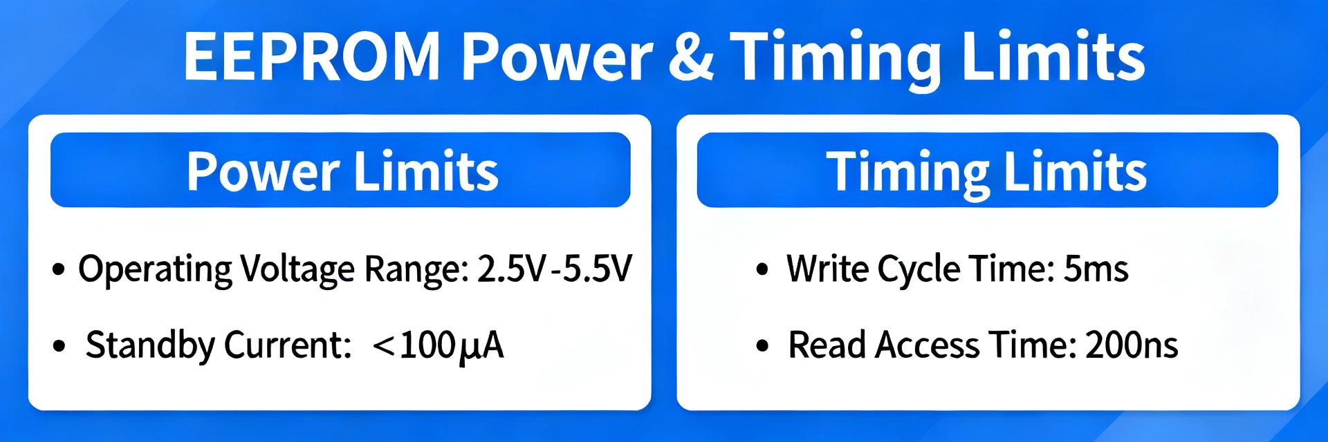
2 — Electrical Characteristics: Supply & Currents
| Parameter | Symbol | Typical Range | Unit |
|---|---|---|---|
| Supply Voltage (Parasitic) | VCC | 1.7 to 3.6 | V |
| Standby Current | ISB | < 3.0 | µA |
| Active Read Current | ICC1 | 0.08 to 0.3 | mA |
| Write Pulse Current | ICC2 | 2.0 to 5.0 | mA |
2.1 Supply and I/O Voltage Ranges
Correct supply and pull‑up choices determine reliable logic interpretation. Designers must apply the recommended VCC window and a suitable pull‑up so the device is reliably self‑powered by the bus.
3 — Absolute Maximum Ratings & Limits
3.1 Voltage and ESD Thresholds
Absolute maximums define irreversible damage thresholds. Maintain at least a 20% margin below absolute maxima for supply and IO voltages and include transient suppression to protect against surges.
3.2 Thermal and Storage Limits
Follow recommended peak reflow profiles and avoid repeated thermal cycling near limits to preserve endurance and data retention. Apply derating in high‑ambient environments.
4 — Timing & Signal Integrity
Timing violations are a common source of data corruption. Bench validation should verify setup/hold margins and write recovery. Pull‑up value and bus capacitance determine rise time (τ = RPU × Cbus); choose RPU to meet minimum pulse widths while limiting current.
5 — Integration Checklist
- VCC/RPU Rules: Balance rise time and standby leakage.
- PCB Footprint: Verify pad tolerances and orientation marks.
- BOM Margin: Target 80% of absolute maximum ratings for long-term reliability.
- Validation: Test write peaks and recovery timing on final hardware.
Summary
Reliable integration of the AT21CS01-MCHM10-T requires strict adherence to 1-wire timing and voltage limits. Maintain safety margins, optimize pull-up resistors for bus capacitance, and validate current consumption across temperature extremes.
FAQ
How should a designer verify standby current for the device?
Measure ISB with the device in its idle state on a low‑noise supply, with the bus pulled to the recommended level and with minimal external loading. Use a precision current meter or a shunt with a high‑resolution ADC, keep probe leads short, and confirm across temperature extremes for worst‑case budgeting.
What pull‑up resistor range is suggested for reliable operation?
Choose an RPU that balances rise time and current draw using the RC time constant with estimated bus capacitance. Start within the manufacturer’s recommended range, validate logic threshold crossings at worst‑case capacitance and temperature, and reduce value only if timing violations appear.
What are quick diagnostics for intermittent read failures?
Check mechanical contacts and connector resistance first, then measure pull‑up voltage at the device pin during communication. Verify timing margins and probe for noisy power rails or ground bounce. Capture waveforms to isolate protocol timing violations versus physical layer issues.
What safety margin is recommended for absolute maximum ratings?
It is best practice to maintain at least a 20% safety margin below the absolute maximum voltage and temperature ratings specified in the datasheet to account for power supply transients and environmental fluctuations.