גיליון נתונים S-19190AIH-M6T1U: ניתוח מעמיק של מפרטים עיקריים ומגבלות
Introduction
Point: The device monitors one Li‑ion cell in a compact SOT‑23‑6 footprint with automotive‑grade environmental range, defining where it can be applied and how it must be validated. Evidence: the datasheet lists single‑cell support, SOT‑23‑6 package and an operating temperature range from −40°C to +105°C. Explanation: these baseline numbers set expectations for thermal management, PCB layout and qualification scope when evaluating fit for automotive or harsh‑environment designs.
(1) Product overview & intended applications — background introduction
What the device is and its core functions
Point: At its core the IC is a voltage monitor and protector for a single Li‑ion cell with limited cell‑balancing/control features. Evidence: datasheet headings and pin descriptions indicate sense and control pins for over‑/under‑voltage detection and status signaling. Explanation: designers should treat it as a front‑end monitor—suitable for threshold detection, fault signalling and basic cell management rather than full BMS functionality.
Target application domains & conservative use-cases
Point: Best use is in compact battery packs, small BMS front‑ends and sensing nodes where size and automotive qualification matter. Evidence: SOT‑23‑6 and the −40°C to +105°C rating imply automotive/industrial readiness. Explanation: conservative deployments include single‑cell portable power modules and vehicle accessory nodes; avoid high‑power stacks or systems requiring active balancing unless paired with dedicated balance circuitry and thermal headroom.
(2) Datasheet electrical specs: voltage, thresholds and accuracy — data analysis
Supply, detection thresholds and tolerance
Point: The datasheet defines VCC operating window, OV/UV trip points and accuracy bands as separate typical vs guaranteed columns. Evidence: threshold tables separate typical, min/max and temperature‑dependent columns and list hysteresis/blanking parameters. Explanation: read the guaranteed column for pass/fail criteria; use typical values for initial bench expectations but design margins around worst‑case tolerances and temperature shifts shown in the specs.
Time-related specs: response, debounce, and detection timing
Point: Detection speed is shaped by internal filtering, blanking and specified response times—tradeoffs between transient immunity and latency. Evidence: timing table gives debounce/blanking intervals and minimum detection delay entries. Explanation: validate with rail transient tests using step and pulse waveforms that match or exceed datasheet test conditions to confirm immunity without masking legitimate faults.
(3) Thermal & environmental limits — data analysis / limits
Operating and storage temperature + derating guidance
Point: The −40°C to +105°C operating range is a primary deployment limiter; storage and absolute max extend beyond. Evidence: the datasheet lists operating and storage ranges separately and provides thermal resistance (θJA) guidance. Explanation: for continuous high‑temperature use derate supply and verify junction rise with thermal simulation; expand copper pour and add vias to reduce θJA and protect against thermal overstress in sustained operation.
Reliability & qualification notes (AEC-level implications)
Point: Automotive qualification flags imply extended test coverage but do not remove need for supplier verification. Evidence: datasheet qualification notes indicate device meets automotive test vectors and lot acceptance criteria. Explanation: treat the flag as a baseline—still require incoming inspection, lot‑by‑lot sampling and system‑level qualification to ensure assembly, soldering and PCB stresses preserve device reliability.
(4) Package, pinout and PCB/layout considerations — method / design guide
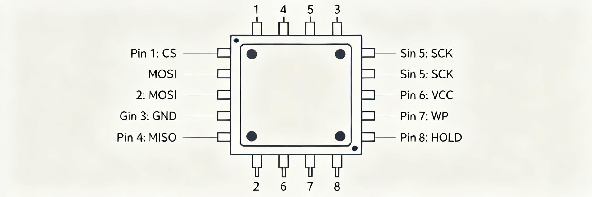
Pin functions and typical connection diagram
Point: Pins map to VCC, sense, ground and control/status lines; decoupling and short sense traces are essential. Evidence: pin table and recommended connection diagram show decoupling cap close to VCC and sense resistor placement near the sense pin. Explanation: place the decoupling capacitor within 1–2 mm of VCC, keep sense traces <5 mm and use Kelvin routing where practical; add test pads for sense, VCC and STAT to support bench validation.
Thermal layout, copper pours and assembly notes
Point: SOT‑23‑6 thermal behavior depends on PCB copper, via arrays and solder fillet. Evidence: θJA guidance and recommended land patterns appear in the mechanical/thermal notes. Explanation: use large thermal pours on ground, add thermal vias under the package area, avoid copper keepouts that isolate the pad thermally and follow recommended reflow profile to ensure consistent solder fillet and thermal transfer.
(5) Limits, failure modes & test checklist — method / actionable analysis
Electrical overstress and protection limits
Point: Absolute maximum ratings set the ESD, input voltage and reverse voltage limits; violating them leads to latch‑up or permanent damage. Evidence: absolute‑max table lists input clamps, ESD classification and reverse‑polarity notes. Explanation: mitigate risk with series resistors, small TVS/clamp diodes, and input current limiting; add layout features that prevent large capacitive discharge into sense pins during assembly or fault events.
Test checklist for lab validation
Point: A focused lab plan validates thresholds, timing, thermal and transient robustness. Evidence: use datasheet test conditions as pass/fail references for OV/UV levels, debounce timing and thermal behavior. Explanation: perform supply ramp tests, OV/UV threshold verification with ramps and steps, thermal soak at high‑temp, and transient injection—accept only if measured values remain within guaranteed limits plus design margin.
(6) Example integration & design checklist — case study + action suggestions
Example single-cell monitor integration (concise case)
Point: A minimal integration includes the monitor, a sense resistor, decoupling and a status indicator. Evidence: component list commonly comprises a 0.01–0.1 Ω sense resistor, 0.1 µF decoupling cap and pull resistors for status pins. Explanation: expect measured thresholds near the datasheet typicals; place scope probes at the sense pin and STAT node to verify trip behavior during controlled over/under excursions and measure quiescent current for power budget.
Final design checklist & go/no-go decision points
Point: A concise checklist prevents late surprises: thermal headroom, accuracy margin, EMC/ESD precautions and procurement quality. Evidence: cross‑check thermal derating, guaranteed accuracy bands and absolute max values from the specs. Explanation: greenlight if margins >20% against worst‑case tolerance, thermal rise <10°C above ambient in expected loading, and incoming parts pass lot acceptance; otherwise iterate design or select alternate component.
| Parameter | Condensed value / note |
|---|---|
| Supported cells | Single‑cell monitor |
| Package | SOT‑23‑6 |
| Operating temp | −40°C to +105°C |
| Key specs | OV/UV thresholds, hysteresis, timing per datasheet tables |
| Absolute max | See datasheet ABS MAX; protect with clamps |
Summary (conclusion & quick reference)
- Single‑cell suitability and compact SOT‑23‑6 package make the monitor ideal for space‑constrained packs; confirm thermal path and copper pour to meet the −40°C to +105°C operating range and thermal derating.
- Thresholds and timing are provided as typical vs guaranteed in the datasheet—use guaranteed numbers for pass/fail and validate with ramp/pulse test waveforms to confirm OV/UV behavior under worst‑case conditions.
- Limit the risk of electrical overstress with series resistance and clamps, perform lot acceptance testing, and ensure design margins exceed datasheet worst‑case tolerances before production use.