


Helping you save cost and time.

Provide reliable packaging for your goods.

Quick and reliable delivery to save time.

Excellent after-sales service.
New Product Launch
More +


Hot Selling Parts


Blog
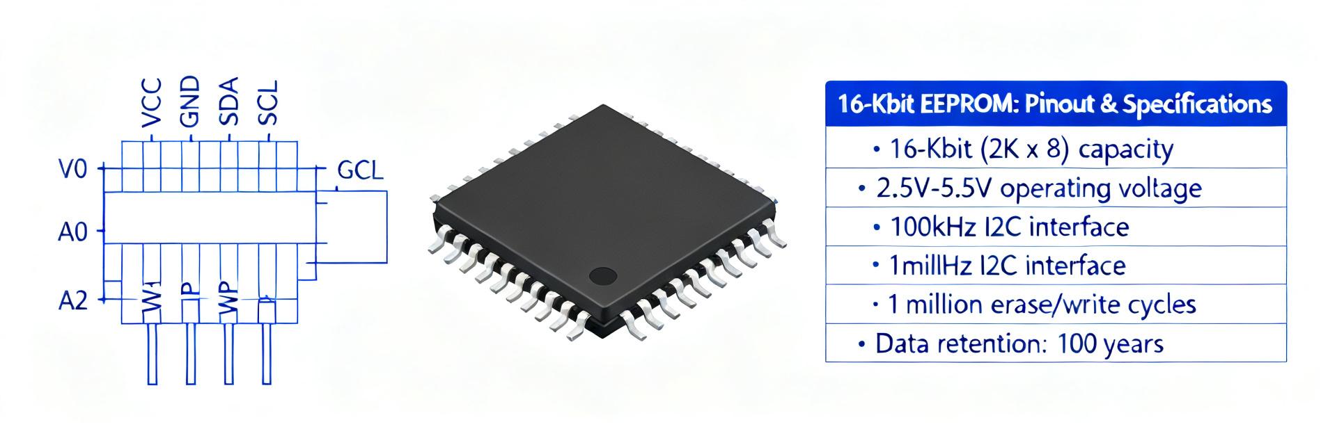
S-93A86BD0A Datasheet: Pinout & Electrical Specs Overview
The S-93A86BD0A is a 16-Kbit serial EEPROM class device commonly used for nonvolatile configuration, calibration and small data logging. Typical electrical specs for quick reference: VCC range 2.5–5.5…
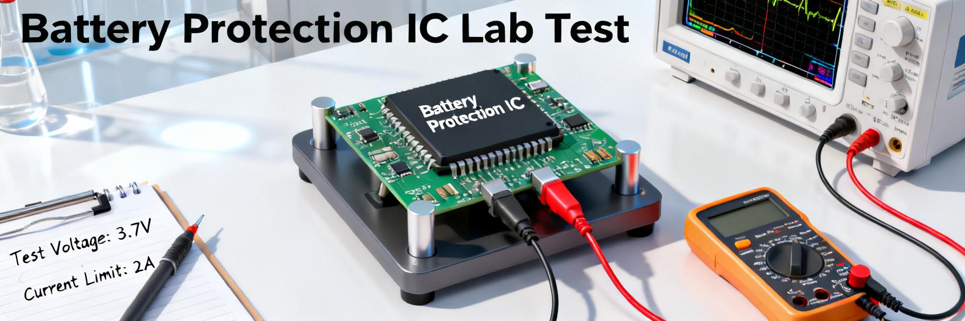
S-8235AAK-TCT1U Specs: Measured Performance Report
In controlled bench tests covering voltage threshold accuracy, overcurrent response and thermal stress, the S-8235AAK-TCT1U delivered repeatable detection and protection behavior—highlighting predicta…
S-19190 Series Reliability Report: Automotive BMS Insights
2026-07-23 10:35:12
S-19190BEH-M6T1U Specs: Key Voltage Monitor IC Metrics
2026-07-22 10:26:10
S-25C640A0H-J8T2U3 datasheet: Complete key specs & pinout
2026-07-21 10:46:11
S-93A76BD0A-J8T2U3 Datasheet: Pinout, Specs & Timing
2026-07-20 10:36:10
S-19190ADH-M6T1U Datasheet Deep Dive: Key Specs & Pinout
2026-07-19 10:35:15
Read more