S-25A080 SPI EEPROM: Benchmark Tests & Read/Write Specs
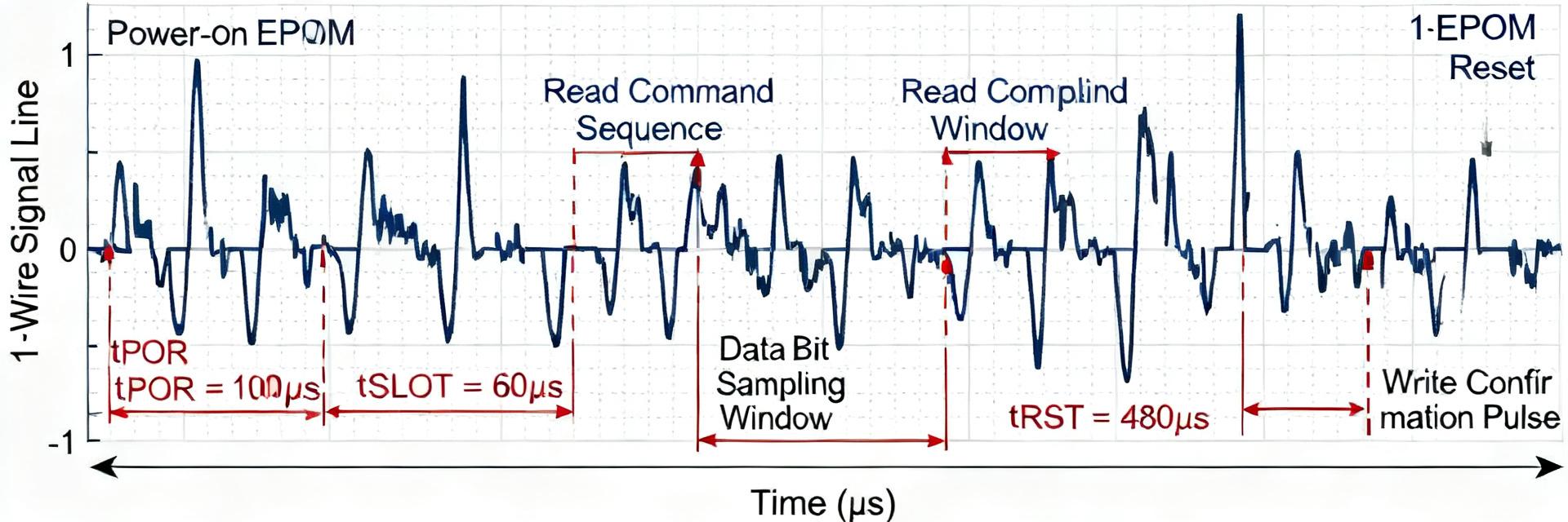
The S-25A080B0A-T8T2U3 is rated in its datasheet as an 8K‑bit, 1K×8 SPI EEPROM with a maximum clock near 6.5 MHz and millisecond‑scale page write cycles; these limits frame a practical benchmark suite to quantify throughput, latency, and power across operating conditions.
1 — Key specs & device overview
The device architecture is optimized for low-power industrial logging where byte-level durability and predictable SPI timing are paramount.
| Field | Value (typical) |
|---|---|
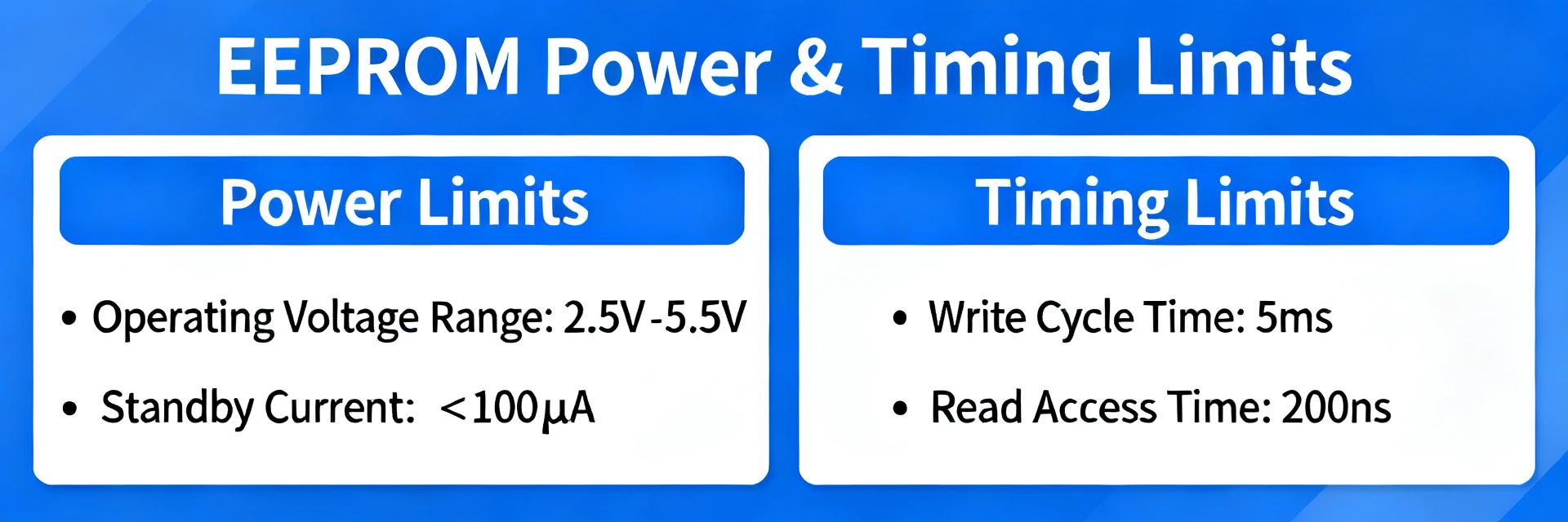
| Memory density | 8 Kbit (1K × 8) |
| Supply (VCC) | 2.5–5.5 V |
| Max SPI clock | ≈6.5 MHz |
| Page size | 16–32 bytes |
| Write cycle (tWC) | Typical 4ms - 10ms |
Protocol basics: SPI commands & addressing
Transactions follow the standard SPI sequence: CS low → opcode → address → data → CS high. Polling the status register is mandatory for efficient write management.
# Pseudocode sequence
CS=LOW; send(WREN_OP); CS=HIGH;
CS=LOW; send(WRITE_OP); send(ADDR); send(DATA_PAGE); CS=HIGH;
while(poll_status() & WIP_BIT);
2 — Read performance: benchmarks & analysis
Read throughput is largely limited by the SPI clock frequency and command overhead. Burst reads demonstrate significantly higher efficiency than random single-byte access.
- First-byte latency: Includes command (8-bit) and address (16-bit) transmission.
- Steady-state: Maximum throughput is achieved during continuous reads at 6.5 MHz.
- VCC Sensitivity: Higher VCC typically allows for cleaner signal transitions and more stable max-clock operation.
3 — Write performance & endurance
Write operations are gated by the internal tWC (Write Cycle Time). Effective throughput drops if the firmware writes single bytes instead of full pages.
- Effective Throughput: Calculated as
Total Bytes / (Write Time + Polling Time). - Endurance: Testing requires cycle logging to monitor for bit-flips or depletion of the charge pump efficiency over 100k+ cycles.
4 — Practical recommendations & troubleshooting
Integration Checklist
- Limit SPI clock to 80% of rated max for high-temperature environments.
- Ensure 0.1µF decoupling is within 2mm of the VCC pin.
- Implement hardware Write Protection (WP) for boot-critical data.
- Always use page-aligned writes to reduce wear and improve speed.
FAQ
How do I verify S-25A080B0A-T8T2U3 read/write correctness in a harness?
Use deterministic patterns (incrementing bytes, 0xAA/0x55), perform a readback immediately after status indicates write completion, and compare checksums. Automate 30+ iterations per condition and log first‑byte latency, steady throughput, VCC, and clock.
What is the best way to measure write throughput for SPI EEPROM?
Run repeated page‑aligned writes while including tWC and polling overhead. Log total data transferred and total elapsed time. Compute effective throughput = total bytes / total elapsed time.
How should firmware handle status register and write retries for reliable writes?
After issuing a page program, poll the status register with short delays and an exponential backoff. Cap retries and log failures for later analysis. Use the hardware WP/HOLD to protect against accidental writes.
What are common failure modes during S-25A080 benchmarks?
Failed writes are often due to missing WREN opcodes or power glitches during the tWC window. Timing issues usually stem from violated CS setup/hold times which can be verified using a logic analyzer.
Summary: The S-25A080B0A-T8T2U3 provides a robust memory solution when page-alignment and status polling are correctly implemented. Use the benchmark methodologies above to ensure system stability across the full automotive/industrial temperature range.