
S-25C040A0H-J8T2UD EEPROM Datasheet: Key Specs & Tests
The S-25C040A0H-J8T2UD is a 4-Kbit serial EEPROM designed for low-density nonvolatile storage in sensor modules, IoT endpoints, and industrial control nodes. This guide summarizes the EEPROM datasheet, highlights the key specs engineers must validate, and provides practical bench tests to confirm endurance, retention, and low-power behavior before production.
Engineers should use the official EEPROM datasheet as the single source for numeric limits and recommended reflow/ESD profiles; this article explains where to look in the datasheet and how to convert listed values into pass/fail test criteria for procurement and qualification.
1 — Product overview & datasheet at-a-glance (background)
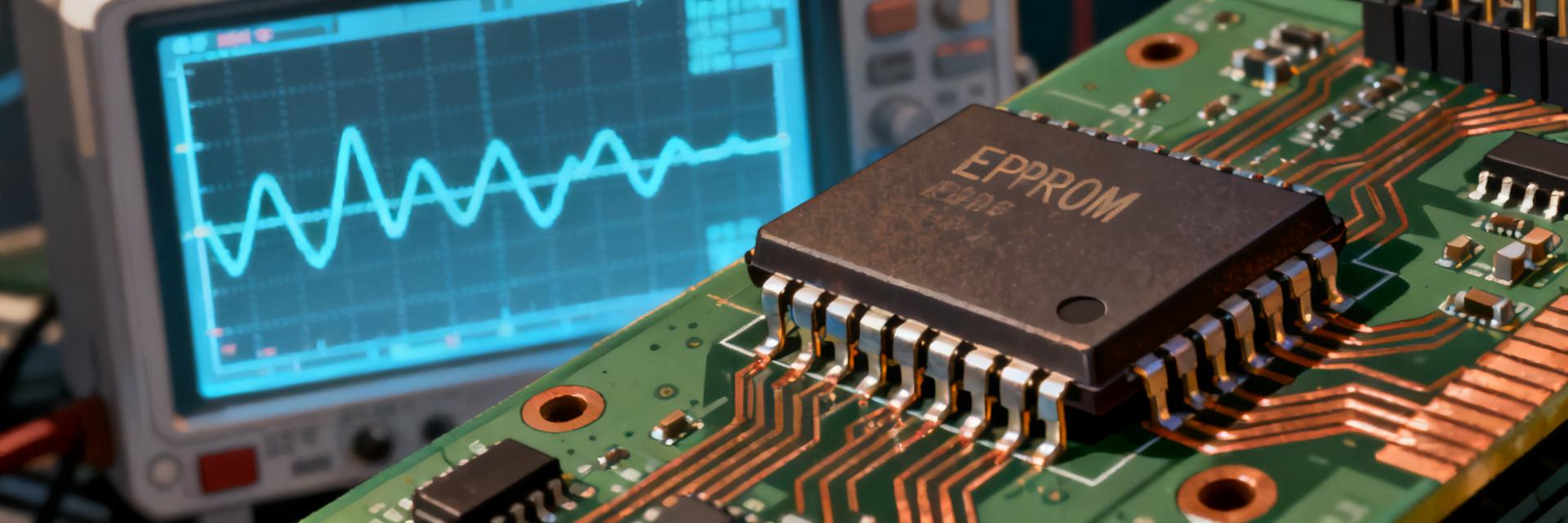
What this part is and where it fits
Point: This part is a byte-addressable serial EEPROM suitable for small persistent stores.
Evidence: The datasheet identifies total bits and organization in the memory-map table.
Explanation: 4 Kbit provides 512 bytes—enough for calibration tables or bootloader flags without the power and cost overhead of larger NVM.
Package, ordering codes & marking summary
Point: Confirm package, temperature grade, and ordering code suffix before ordering.
Evidence: The datasheet lists available packages, package markings, and temperature ranges in the packaging section.
Explanation: Map the ordering code to the package/version on the datasheet; verify pin count and footprint recommended land pattern to avoid board-level surprises.
2 — Key specs & electrical characteristics (data analysis)
Memory organization & density (key specs)
Point: Use the datasheet memory-map table to extract organization, page-size, and address limits.
Evidence: Memory organization and addressing appear in the datasheet section that details memory map and command codes.
Explanation: For embedded firmware, design buffers sized to page boundaries and implement read-modify-write logic when updating fewer than a full page.
Supply, current, and timing budget (electrical characteristics)
Point: Verify supply voltage range, operating/standby currents, and write timing from the electrical characteristics tables.
Evidence: Datasheet electrical tables provide VCC range, typical active/standby currents, and typical/max write times.
Explanation: For battery-powered nodes, confirm standby leakage and write energy; measure write/erase timing on the bench to confirm worst-case throughput and duty-cycle limits.
3 — Interface, command set & timing tests (method guide)
Interface overview & protocol checks
Checklist: Confirm bus mode, clock phase/polarity, chip-select timing, and required pull-ups. Use a logic analyzer to capture command sequences and compare to timing diagrams in the datasheet.
Timing and throughput test procedures
Point: Measure clock frequency tolerance, CS/SS timing, page-write duration, and maximum sustained throughput.
Evidence: Timing diagrams and timing-characteristics tables show min/max delays and cycle times.
Explanation: Test steps: 1) sweep clock up to indicated max and verify reads; 2) measure page-write completion with a scope; 3) perform repeated-write throughput to observe thermal or timing degradations. Pass/fail is whether measured timings fall within datasheet min/max limits.
4 — Reliability, endurance & environmental testing (method guide / data analysis)
Endurance, data retention & lifecycle tests
Procedure: Define accelerated test cadence, log failures, and generate cycles vs. error-rate curves. Report median cycles-to-failure, 95% confidence intervals, and any bit pattern dependencies observed.
Temperature, ESD and soldering profile checks
Point: Follow datasheet limits for operating temperature, reflow profile, and ESD tolerance.
Evidence: Thermal and soldering guidance appear in absolute-maximum and packaging sections.
Explanation: Perform thermal cycling, humidity soak, and ESD bench tests per the datasheet-recommended profiles. Inspect common failure modes: package cracking, solder-fillet issues, and data corruption after thermal stress.
5 — Application examples & comparative guidance (case study)
Typical application scenarios
Profiles: For a sensor node, prioritize low standby current and retention. For bootloader flags, prioritize write atomicity and fast write time. Each profile has a short checklist: address map, write latency, and retention under temp.
Alternative parts checklist (how to compare)
Point: Compare on interface, write time, current draw, and temp grade.
Evidence: Create a spec table with rows for Interface, Density, Page Size, Write Time, Active/Standby Current, Temp Range, and Endurance.
Explanation: Use a consistent checklist schema to compare candidates without supplier names: fill numerical values and mark pass/fail versus system requirements.
| Spec | Decision Criteria |
|---|---|
| Interface | Match MCU peripheral and required bus speed |
| Page size | Align with firmware write patterns |
| Write time | Must support boot or runtime update windows |
| Active/Standby current | Fit battery budget |
| Temp range / Endurance | Meet environmental lifetime goals |
6 — Practical selection & bench-testing checklist (action)
Pre-purchase checklist
- Confirm memory density and organization match application needs.
- Verify package pinout and recommended land-pattern.
- Check operating VCC range and timing limits for MCU compatibility.
- Request datasheet revision and lot/traceability fields for procurement.
Step-by-step bench test script
Power-up checks, ID read, basic read/write/verify, endurance spot-check (e.g., 10k cycles), and environmental spot tests (hot/cold retention). Define measurable pass criteria: all reads match expected values, write times ≤ datasheet max, standby current ≤ datasheet spec, and no bit errors after stress.
Summary
Recap: This overview pairs the S-25C040A0H-J8T2UD EEPROM datasheet summary with actionable test procedures and selection checklists so engineers can validate part suitability quickly. The recommended next steps are to run the bench test script, compare measured results to datasheet limits, and document findings for QA sign-off.
- Confirm memory map and page size from the EEPROM datasheet before firmware integration; align buffers to page boundaries to avoid RMW inefficiencies.
- Measure active and standby current and write timing on the bench; use these values to verify battery-life and throughput claims.
- Perform an endurance spot-check and retention verification under expected temperature extremes to quantify lifecycle margin.
- Validate package, footprint, and reflow profile prior to placement to prevent assembly-level failures and ensure compliance with thermal limits.
Frequently Asked Questions
What are the essential tests to validate the EEPROM datasheet claims?
Run ID read, timing verification (clock/CS margins), page-write timing, active/standby current measurements, short endurance cycles, and retention checks at temperature extremes. Document numeric results and compare them to the datasheet max/min values to establish pass/fail.
How should I interpret page size and address range from the EEPROM datasheet?
Page size dictates atomic write granularity: firmware should write in page-aligned batches or implement read-modify-write when updating smaller regions. Address range (e.g., 0x000–0x1FF for 512 bytes) defines valid offsets—attempts outside that range will fail or wrap depending on device behavior described in the datasheet.
Which failure modes are most common during qualification of low-density EEPROMs?
Common failures include data corruption after thermal cycling, soldering-induced package damage, slow write completion beyond datasheet maxima, and elevated standby leakage. Use the suggested environmental and ESD tests to catch these modes early in qualification.
What is the recommended pre-purchase footprint verification step?
Confirm memory density and organization map directly to firmware requirements, trace ordering suffix codes to identify exact physical packaging, verify the PCB footprint against the manufacturer recommended land pattern, and request lot traceability reports.





