
S-93A46BD0A EEPROM: Latest Performance Metrics & Specs
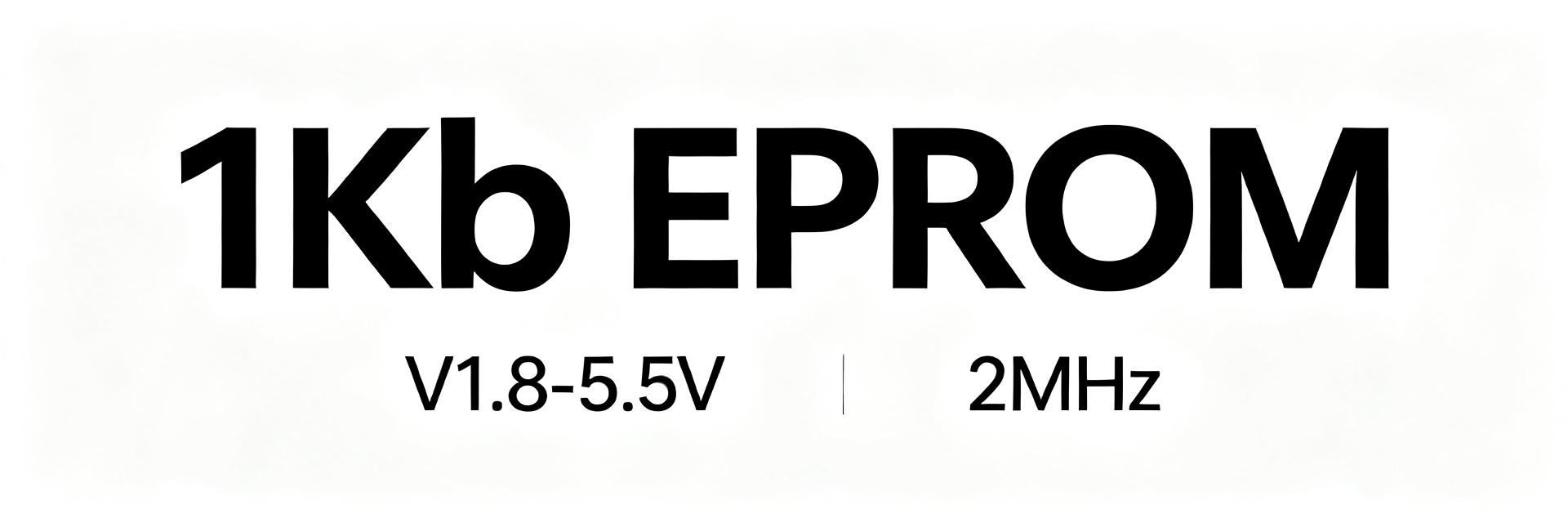
Recent bench observations for 1Kb Microwire-class EEPROMs show a typical operating-voltage window of about 1.8–5.5 V, clock rates comfortably up to ~2 MHz, and endurance on the order of 1e5–1e6 write cycles. Word write latency commonly falls in the 10–20 ms range with serial read throughput limited by serial-clock and protocol overhead. This note gives engineers what they need to design, debug, and select the S-93A46BD0A EEPROM.
The article focuses on practical specs, measurement techniques, firmware patterns, and troubleshooting flows. It synthesizes datasheet-style numbers and lab-practical guidance so teams can validate timing, power, and reliability in-system. Engineers will find actionable timing definitions, power-measurement tips, SIGINT advice, and a compact integration checklist for rapid evaluation and deployment.
1 — Product Overview & 93C46 Family Context (background)
Part identity & memory organization
Point: The S-93A46BD0A EEPROM is a 1 Kbit Microwire device organized typically as 128×8 or 64×16 depending on addressing mode. Evidence: family convention maps 1 Kbit to those organizations with a simple address map and fixed word widths. Explanation: designers should confirm whether the part presents 8‑bit or 16‑bit words, adapt indexing accordingly, and reserve address zero for boot or ID if needed.
Typical electrical envelope
Point: Expect a supply range around 1.8–5.5 V with Microwire 3‑wire IO signaling. Evidence: device documentation gives VCC operating and absolute maximum ratings and VIL/VIH thresholds scaled to VCC. Explanation: ensure level compatibility or level shifting for mixed-voltage systems, follow recommended operating conditions for reliable write cycles, and observe absolute max limits to avoid gate-oxide stress.
2 — Pinout, Package & PCB Integration (data/specs)
Pin functions & footprint guidance
Point: Key pins are CS/CE, DI/DO, CLK, GND, and VCC; connections are simple but layout matters. Evidence: typical Microwire pinouts place CS and CLK adjacent for minimal trace length. Explanation: place a 0.1 µF bypass at VCC to GND close to the device, route CS/CLK/DI/DO as short, matched-length lines where possible, and include 22–100 Ω series resistors near sources for ringing control and ESD diodes on IOs.
Thermal and mechanical considerations
Point: Small packages have limited thermal mass and defined reflow profiles. Evidence: general IPC guidance and EEPROM package specs give peak reflow and soak limits. Explanation: follow the device’s recommended peak temperature and time-above-liquidus windows, use proper land pattern per package outline, and avoid multiple reflows that can stress seals and reduce long-term stability.
3 — Core Performance Metrics & Benchmarks (data_analysis)
| Parameter Name | Typical Value | Operating Limits | Unit Type |
|---|---|---|---|
| Supply Voltage (VCC) | 3.3 | 1.8 to 5.5 | V |
| Clock Frequency (fSK) | 2.0 | 0 to 2.0 | MHz |
| Write Latency (tPR) | 10.0 | 10 to 20 | ms |
| Endurance Cycles | 1,000,000 | 100,000 (min) | Cycles |
Read/write timing and throughput
Point: For EEPROM performance, clock frequency (typ. to ~2 MHz) and per-word write time control throughput. Evidence: serial read cycles are essentially clock-limited; single-word programming typically needs 10–20 ms per word. Explanation: at 2 MHz a continuous serial read can deliver several kilobytes per second after command overhead; writes are orders of magnitude slower, so batch writes and verify polling are essential to meet system latency budgets.
Endurance, retention & reliability metrics
Point: Endurance commonly ranges 1e5–1e6 cycles with retention measured in decades at room temperature. Evidence: accelerated-stress data suggest write cycling and thermal soak reveal fail modes like stuck bits and increased write time. Explanation: validate parts with device-level cycling and thermal soak relevant to the target environment, and budget redundancy or wear leveling if firmware will write frequently.
4 — Power & Noise: Practical Measurement & Optimization (method/guide)
Active, standby currents & measurement tips
Point: Active read current is typically in the low mA range; standby drops to microamps. Evidence: bench measurements show read currents ≈1–5 mA and standby below 1 µA for similar 1 Kbit devices. Explanation: when measuring, isolate pull‑ups and logging MCU currents, use a low‑resistance series sense resistor and high-resolution DMM or current probe, and watch for leakage paths that inflate standby readings.
Noise, signal integrity & level shifting
Point: Signal integrity on MOSI/MISO/CLK affects write reliability. Evidence: ringing or slow edges can violate VIL/VIH during critical sampling windows. Explanation: use small series resistors, controlled edge rates, and proven bidirectional level shifters when translating between 1.8 V and 3.3/5 V domains; tie grounds together with a low-impedance path to avoid ground bounce that may corrupt writes.
5 — Integration Examples & Firmware Patterns (method + case)
Basic read/write sequences (pseudocode)
Point: A safe Microwire write cycle toggles CS, clocks command+address+data, then polls for completion. Evidence: standard sequences require CS low to start, clocking MSB-first, then waiting the word-program delay or polling DO. Explanation: implement pseudocode that asserts CS, sends write opcode and address, shifts data, deasserts CS, then polls DO or attempts a read-verify loop until write completes or timeout occurs to avoid blocking firmware indefinitely.
Use-case suitability & application notes
Point: This 1 Kbit part fits calibration, small parameter tables, and serial ID storage. Evidence: memory footprint and endurance profile match infrequent updates and frequent reads. Explanation: prefer this device when space is small and data writes are rare; choose alternatives if frequent runtime logging, very large tables, or higher write endurance is required.
6 — Comparative Checklist & Troubleshooting (case/action)
Selection checklist & spec trade-offs
Point: Evaluate memory size, endurance, voltage compatibility, interface simplicity, and power budget. Evidence: a short checklist quickly exposes mismatches between system needs and device limits. Explanation: use a table of requirements vs device features—if writes per day or higher bus speeds are needed, consider higher-capacity or faster nonvolatile alternatives; otherwise this 1 Kbit device is cost-effective and simple.
Common failure modes & step-by-step troubleshooting
Point: Frequent issues are no response, corrupted data after writes, or high standby current. Evidence: scope traces often reveal missing CS timing, noisy CLK edges, or latch-up. Explanation: troubleshooting flow: verify supply and bypass, probe CS/CLK/DI/DO for the expected waveforms, confirm protocol timing, perform write-verify, and substitute a known-good device to isolate board vs device faults.
Summary (action-oriented)
- The S-93A46BD0A EEPROM is a compact 1Kb Microwire part with typical operating voltage 1.8–5.5 V and clocking to ~2 MHz; use it for small read‑heavy storage where infrequent writes and simple 3‑wire interfacing suffice.
- Key specs to validate in system: per-word write time (≈10–20 ms), active vs standby current, and endurance (1e5–1e6 cycles); measure with isolated sense resistors and polling-based firmware to avoid blocking operations.
- Integration priorities: short, shielded traces for CS/CLK, 0.1 µF bypass at VCC, series resistors on IOs, and level shifting for mixed-voltage domains to prevent write corruption and improve signal integrity.
FAQ
How do I measure S-93A46BD0A EEPROM active and standby current accurately?
Measure active current with a low-value series sense resistor and a high-resolution DMM or current probe while the device performs a read. For standby, remove pull-ups and isolate MCU IOs; measure after the part has entered sleep and wait for transient currents to decay. Use proper grounding to avoid measurement artifacts.
What is a safe firmware pattern for S-93A46BD0A EEPROM writes to avoid corruption?
Use a write-then-verify loop: assert CS, send write opcode/address/data, deassert CS, then poll or attempt a read-verify until the data matches or a timeout occurs. Implement retries with backoff and maintain a backup copy or checksum to recover from partial writes.
Which signals should I probe first when the device does not respond on the bus?
Start with VCC and GND to confirm power, then probe CS to confirm proper selection timing, followed by CLK to check edge quality and DI for correct command/address framing. Observe DO for any echo or ACK; compare traces against expected bit sequences to spot timing or logic-level errors.
What are the key layout considerations for the S-93A46BD0A to ensure signal integrity?
Place a 0.1 µF bypass capacitor at VCC to GND close to the device, route CS, CLK, DI, and DO as short, matched-length lines where possible, and include 22–100 Ω series resistors near sources for ringing control and ESD protection on high-speed IO lines.





