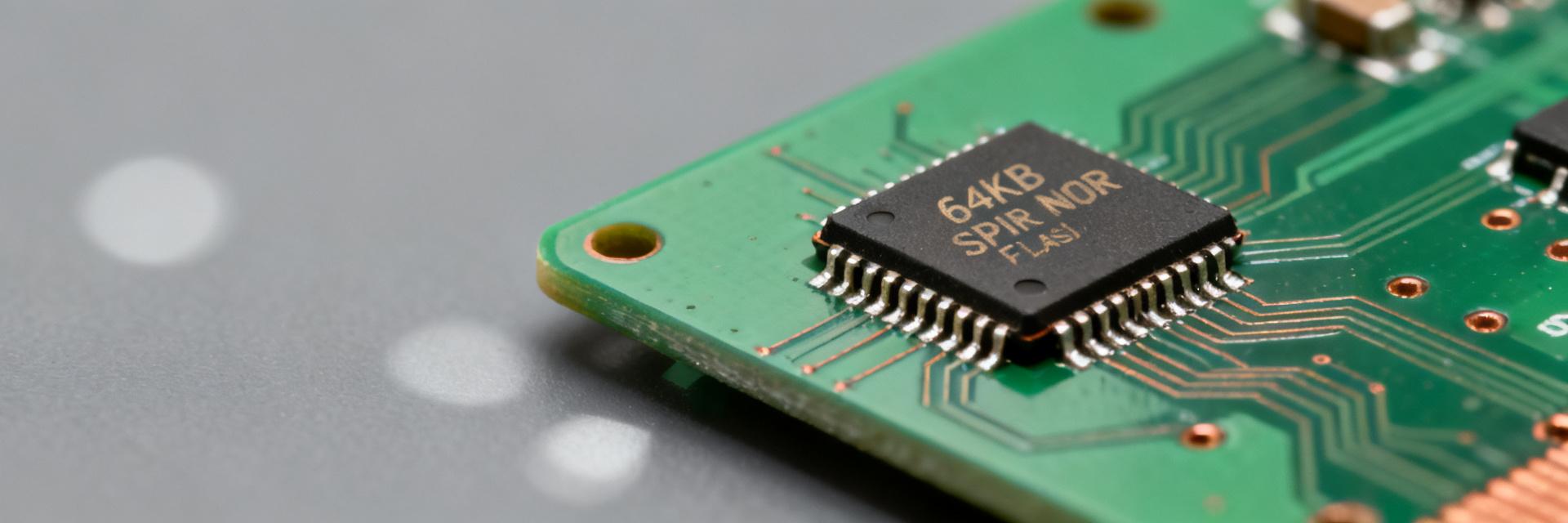
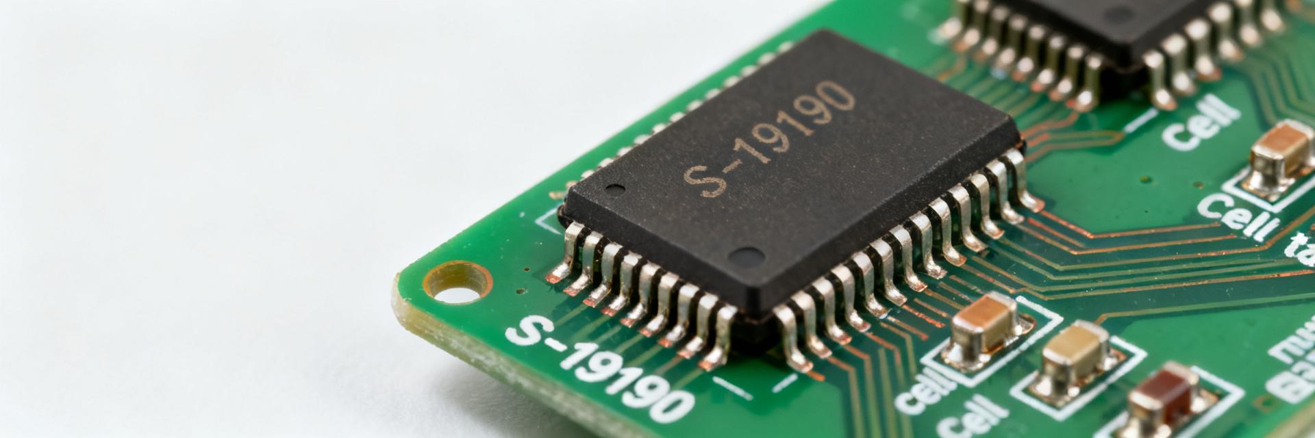
2ED2772S01GXTMA1: Quick Specs & Performance Summary
Key Takeaways (Core Insights)
- Ultra-Low Standby: 85 μA quiescent current maximizes efficiency in battery-powered idle states.
- High-Speed Switching: 90 ns propagation delay enables higher PWM frequencies for smaller magnetics.
- Space Efficiency: VSON-10 package reduces PCB footprint by ~30% compared to standard SOIC-8 drivers.
- Thermal Robustness: 2W power dissipation capability supports demanding high-load motor control.
The 2ED2772S01GXTMA1 is a precision half-bridge gate driver engineered for modern power stages. By balancing a tight 90 ns propagation delay with a remarkably low 85 μA quiescent current, it provides engineers with the ability to design high-density motor drives and DC-DC converters without compromising on thermal efficiency or board space.
1. Strategic Benefits & Real-World Utility
Technical specifications are only as good as the problems they solve. Here is how the 2ED2772S01GXTMA1 translates numbers into system-level advantages:
- 95% Topology Efficiency: The low propagation delay minimizes dead-time requirements, reducing body diode conduction losses in synchronous rectification.
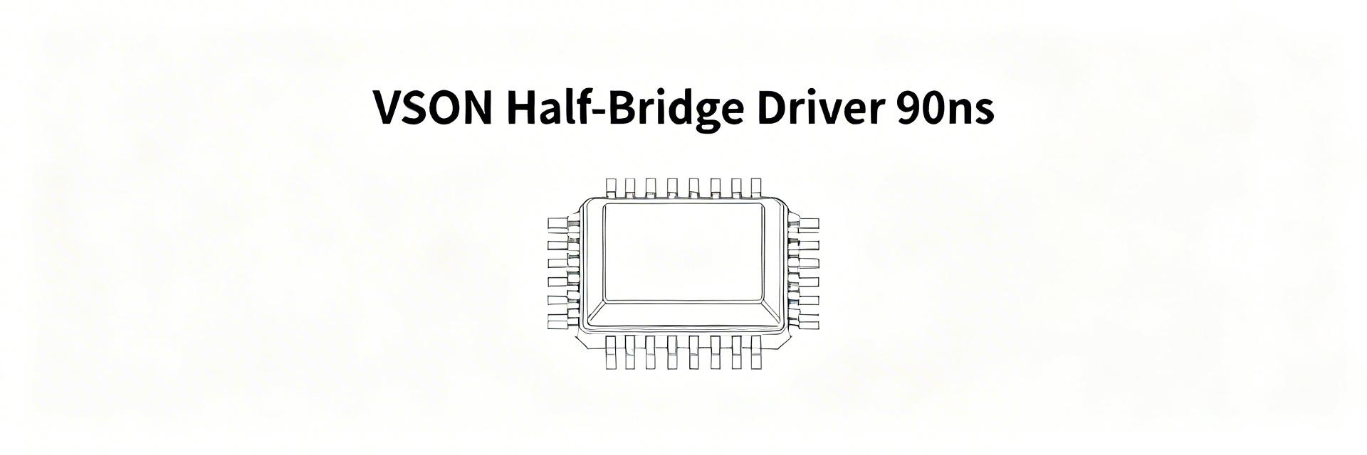
- Compact Form Factor: The VSON-10 package features an exposed thermal pad, allowing for a 2W dissipation in a footprint smaller than a fingernail.
- Battery Longevity: The 85 μA quiescent current is ideal for "Always-On" IoT power tools and e-mobility applications.
2. Professional Competitive Comparison
How does the 2ED2772S01GXTMA1 stack up against industry standards?
| Feature | 2ED2772S01GXTMA1 | Generic 600V Driver | User Benefit |
|---|---|---|---|
| Prop. Delay | 90 ns (Max) | 120-150 ns | Faster switching/Lower EMI |
| Quiescent Current | ~85 μA | ~150-300 μA | Higher Light-Load Efficiency |
| Package | VSON-10 (Thermal Pad) | SOIC-8 | Superior Heat Dissipation |
| Logic Interface | TTL/CMOS (3.3V/5V) | Fixed 5V | Direct MCU Interfacing |
🛡️ Engineer’s Insight: Layout & Reliability
By: Jonathan Sterling, Senior Power Electronics Consultant
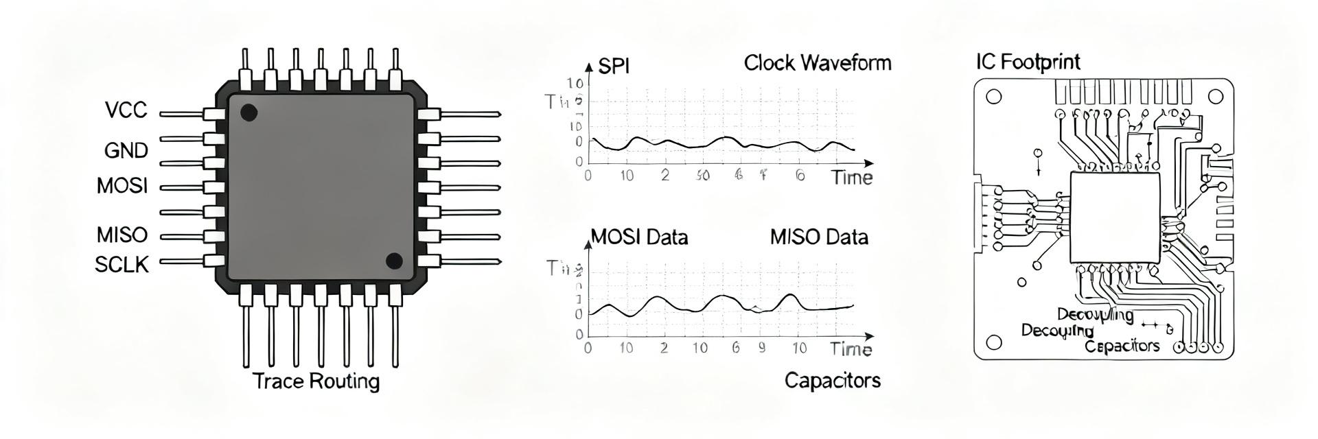
PCB Layout Tip: When using the VSON-10 package, the thermal pad isn't just for heat—it's your electrical anchor. Ensure at least 4-6 thermal vias (0.3mm) connect the pad to a internal ground plane. This reduces the parasitic inductance that causes "ringing" on the gate signal during high-speed transitions.
Selection Pitfall: Don't overlook the 90ns delay when setting your MCU dead-time. While fast, you must account for the mismatch between high-side and low-side channels to prevent catastrophic shoot-through during temperature extremes.
3. Typical Application Visualization
Hand-drawn schematic representation, not a precise circuit diagram (手绘示意,非精确原理图)
Top Use-Cases:
- Class-D Audio: Minimizing THD through precise timing.
- BLDC Motor Drives: Ideal for cordless power tools.
- Micro-Inverters: Maximizing energy harvest in solar apps.
4. Integration & Design Checklist
Critical Validation
- Verify VCC decoupling capacitor is
- Check Bootstrap diode recovery time (Trr
Performance Optimization
- Use Kelvin-source sensing for high-current loops.
- Select gate resistors to control dV/dt vs. losses.
FAQ
Q: What happens if I exceed the 2W power dissipation?
A: The device may enter thermal shutdown or experience accelerated aging. Always validate your junction temperature ($T_j$) using $T_j = T_a + (P_d \times \theta_{ja})$.
Q: Is it compatible with 3.3V microcontrollers?
A: Yes, the logic interface is TTL/CMOS compatible, allowing direct connection to most ARM Cortex-M and ESP32 series MCUs.
Ready to integrate the 2ED2772S01GXTMA1?
Consult the official datasheet for final pinout configurations and absolute maximum ratings.