
S-25C080A0H-T8T2UD Full Datasheet: Pinout, Timing, Specs
The S-25C080A0H-T8T2UD is an 8-Kbit (1,024-byte) SPI serial EEPROM organized as 1K × 8 bytes (16 blocks × 64 bytes); typical page/block-aware write cycles complete in up to 4 ms and the device supports clock rates up to about 6.5 MHz at higher VCC (conservative 5 MHz at lower VCC). This condensed datasheet-style guide gives you the essential numbers and the pinout and datasheet-style guidance you need to evaluate or prototype rapidly.
(1) Overview & Key Specifications for S-25C080A0H-T8T2UD
Memory organization & capacity
Point: The device capacity and organization directly determine addressing and multi-byte write behavior. Evidence: The part contains 8 Kbit total, presented as 1,024 bytes and commonly segmented into 16 blocks of 64 bytes each. Explanation: You address it as byte addresses 0x000–0x3FF; multi-byte writes that cross a 64-byte block boundary will typically wrap or be limited to the remainder of the current block, so you must align multi-byte writes to block/page boundaries or split them to avoid unintended wrapping.
Electrical ratings & operating ranges
Point: Supply and current characteristics set interface constraints and timing capability. Evidence: The device operates across a low-voltage VCC window (device-mode dependent) with maximal clock capability rising with VCC; standby/read currents are microamp-class while write cycles draw higher transient current during tWC. Explanation: Use conservative SCLK limits (≈5 MHz at lower VCC, up to ≈6.5 MHz at elevated VCC), decouple VCC near the pin with a 0.1 μF ceramic and add a 1 μF bulk cap; follow the datasheet test conditions when timing matters and budget transient write currents in power sequencing and regulator headroom.
(2) Pinout & Package Details for S-25C080A0H-T8T2UD
Pin-by-pin signal definitions
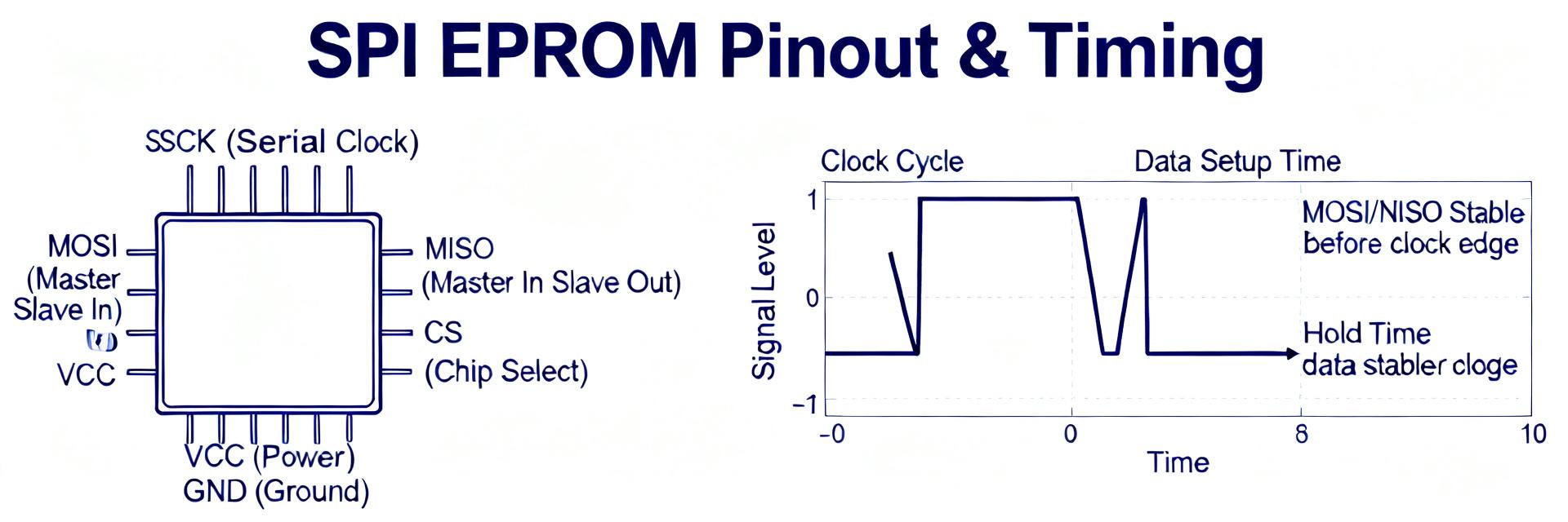
Point: Correct pin wiring and default states prevent communication and protection faults. Evidence: Typical 8-TSSOP pin mapping for 8-pin SPI EEPROMs includes CS# (active low chip select), SO (MISO), WP# (write protect, active low), VCC, SCLK, SI (MOSI), HOLD# (active low), and GND; inputs normally require defined pull-ups or pull-downs depending on active polarity. Explanation: Tie WP# and HOLD# to inactive levels through weak pull-ups if unused; ensure CS# is high when idle. Configure input thresholds per VCC domain and use level translation if domains differ.
| Pin | Name | Type | Notes |
|---|---|---|---|
| 1 | CS# | Input (active low) | Chip select, idle high |
| 2 | SO | Output | Serial data out (MISO) |
| 3 | WP# | Input (active low) | Write protection; pull high to disable |
| 4 | VCC | Power | Decouple close to pin |
| 5 | SCLK | Input | Clock input |
| 6 | SI | Input | Serial data in (MOSI) |
| 7 | HOLD# | Input (active low) | Pause serial clock when asserted |
| 8 | GND | Power | Ground |
Mechanical drawing & footprint notes
Point: Footprint and assembly choices impact solder quality and thermal performance. Evidence: For 8-TSSOP, typical land pattern guidelines call for controlled solder fillets, proper paste aperture reduction and a thermal stable pad arrangement; manufacturer-recommended stencil apertures and solder mask expansion improve yields. Explanation: Place the 0.1 μF decoupler adjacent to VCC and GND pads, avoid large copper pours beneath the part that can cause tombstoning without thermal relief, and follow IPC land-pattern guidance for pad sizes and solder paste percentage to ensure consistent solder fillet and fillet wetting.
(3) Timing, Command Sequences & Example Transactions
Critical timing parameters & SPI modes
Point: Timing parameters control reliable SPI exchanges and write sequencing. Evidence: Key parameters include tWC (write cycle time, up to ~4 ms max typical), SCLK maximum (≈5–6.5 MHz dependent on VCC), and basic setup/hold windows for CS and data. Explanation: Use SPI Mode 0 (CPOL=0, CPHA=0) unless the datasheet specifies otherwise; wrong mode will shift sampling edge and produce framing errors. Respect tWC by polling the status register after a WRITE rather than issuing new writes immediately.
| Parameter | Typical/Max | Notes |
|---|---|---|
| tWC | ≤ 4 ms | Write cycle completes internally |
| SCLK max | ≈5–6.5 MHz | Depends on VCC; use conservative lower rate for reliability |
| SPI mode | Mode 0 | CPOL=0, CPHA=0 typical |
Read/write command flow & example byte sequences
Point: Command sequences and opcodes are the functional API for the device. Evidence: Common opcodes include WREN (0x06), WRITE (0x02), READ (0x03), and RDSR (0x05); sample flow: assert CS#, send WREN (0x06), deassert CS#, assert CS# again, send WRITE (0x02) + 16‑bit address + data bytes, deassert CS#, then poll RDSR until the write-in-progress bit clears. Explanation: Always issue WREN before any write and respect block/page boundaries when constructing multi-byte WRITE sequences.
| Opcode | Function | Minimal notes |
|---|---|---|
| 0x06 | WREN | Set write enable latch |
| 0x02 | WRITE | Address + data; limited by block size |
| 0x03 | READ | Address + continuous read out |
| 0x05 | RDSR | Read status register for WIP bit |
(4) Design Integration & Best Practices
Power sequencing, decoupling & level translation
Point: Stable VCC and proper sequencing avoid device latch-up and mis-programming. Evidence: Recommended decoupling is a 0.1 μF ceramic close to VCC and a 1 μF bulk cap nearby; if interfacing to higher- or lower-voltage logic, level shifters are advised unless the device is explicitly specified as 5 V tolerant. Explanation: Power up the EEPROM after noisy power rails settle if possible; if forced, hold CS# high during power transitions and ensure WP#/HOLD# are pulled inactive to avoid inadvertent protection or bus freeze.
PCB layout, signal integrity & EMI considerations
Point: Routing and termination influence signal integrity at multi-MHz SPI rates. Evidence: Keep CS and SCLK traces short, route SI/SO with controlled-length and avoid stubs; a small series resistor (22–47 Ω) on SCLK can damp reflections. Explanation: Place bypass capacitors close to power pins, add ESD protection at exposed headers, and route high-speed SPI away from sensitive analog traces to minimize crosstalk and EMI coupling in production designs.
(5) Troubleshooting, Test Procedures & Production Checklist
Common failure modes & diagnostics
Point: Recognizing failure signatures speeds root-cause analysis. Evidence: No SPI response can indicate wrong CS polarity, missing ground, or blown device; corrupted reads after write often signal write-wrap across block boundaries or insufficient polling of tWC; persistent write protect indicates WP# active. Explanation: Use an oscilloscope to confirm CS timing and clock edges, read the status register to check WIP and WEL bits, and try a WREN + WRITE + RDSR poll sequence to validate basic programming functionality.
Recommended validation & production test vectors
Point: A small set of deterministic tests verifies device health across production. Evidence: Include: 1) Read device ID/signature if available, 2) Full memory bulk read, 3) Page-aligned write/verify patterns that cross and stop at block boundaries, 4) Endurance stress by repeated write/erase cycles and retention spot checks. Explanation: Automate pass/fail criteria (e.g., single-bit ECC threshold, write-verify mismatch count) and log tWC and status register behavior for early detection of assembly or handling damage.
Summary
Recap: This concise reference concentrates the most actionable numbers and practices for rapid evaluation: memory organization (1,024 bytes in 16 × 64-byte blocks), write-cycle timing (tWC up to ≈4 ms), SPI-mode basics (Mode 0), pin defaults and recommended decoupling, and practical PCB/layout and test vectors. Use this condensed guide — pinout, timing, and integration checklist — as your quick reference when evaluating or integrating the device into prototypes or production boards.





