
S-19190AAH-M6T1U Performance Report: Voltage & Balancing
Bench testing across temperature and load profiles reveals measurable differences in voltage tracking precision and cell balancing responsiveness — critical metrics for reliable multi‑cell packs. This report presents a practical roadmap for validating sensing accuracy and balancing behavior using controlled procedures, focusing on reproducible metrics engineers can use during design and verification.
Datasheet guidance and bench evidence inform test selection and expected ranges for voltage error and balancing current; the procedures below translate those specifications into actionable measurements for component selection and system integration with emphasis on thermal and transient conditions.
Background & Device Overview
Functional role in battery systems
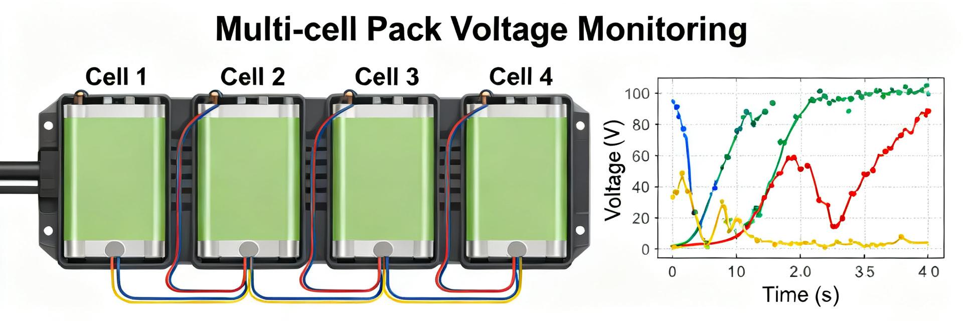
Point: The device functions as a multi‑cell voltage monitor with built‑in cell balancing support. Evidence: Datasheet descriptions identify per‑cell voltage detection, threshold comparators, and passive balancing outputs. Explanation: In system use it supervises single cells, monitors stacks as a companion to a central BMS, and provides safety cutoffs for overvoltage detection while offering resistor‑shunt balancing to reduce cell mismatch.
Key specification areas to evaluate
Point: Critical specs determine real‑world utility. Evidence: Key parameters include detection thresholds, absolute accuracy/tolerance, blanking/delay times, balancing method and per‑channel balancing current capability. Explanation: Extracting those values lets you predict detection V_error, balancing time constants, thermal dissipation, and suitability for automotive/industrial thermal envelopes and package power handling during continuous balancing events.
Test Setup & Methodology
Test hardware, cell selection and environmental conditions
Point: Appropriate hardware and sample selection underpin repeatable results. Evidence: Use representative Li‑ion pouch or prismatic cells, a controlled thermal chamber, precision DMM, oscilloscope, and programmable electronic loads. Explanation: Test at matched and intentionally mismatched initial voltages, run a statistically significant sample size with repeated runs per temperature point, and log ambient and board temperatures to correlate thermal effects with voltage tracking and balancing performance.
Test procedures and primary metrics
Point: Structured tests yield comparable metrics. Evidence: Define static open‑circuit voltage accuracy, threshold trip testing, step‑load transients, balancing activation, and endurance tests. Explanation: Record V_detection, V_error (mV), balancing current (mA), activation delay (ms–s), quiescent current, time‑to‑balance, and energy dissipated. Consistent timing and load profiles ensure meaningful comparisons across devices and firmware states.
| Evaluation Parameter | Expected Range | Test Conditions |
|---|---|---|
| Overcharge Detection (V_DET1) | 3.50 V to 4.60 V (±20 mV) | T_a = -40°C to +85°C |
| Balancing Detection Threshold | 3.40 V to 4.50 V (±25 mV) | T_a = +25°C |
| Detection Delay Time | 0.25 s to 4.00 s (±30%) | C_delay = 0.1 μF |
| Quiescent Current (Active) | 10.0 μA max | V_cell = 3.5 V, no load |
Voltage Performance Analysis
Accuracy across temperature and state of charge (SOC)
Point: Temperature and SOC shift measured voltage accuracy. Evidence: Plot V_error versus temperature and versus SOC to reveal systematic offsets or increased noise at extremes. Explanation: Expect drift trends; use device blanking/delay specs to separate slow systematic offsets from transient noise, and set pack top‑of‑charge detection margins to avoid false overvoltage trips driven by temperature‑induced offsets.
Transient response under load and common‑mode conditions
Point: Load steps and common‑mode shifts challenge sensing. Evidence: Execute step‑load tests while capturing transient overshoot/undershoot and recovery on scope channels referenced to sense nodes. Explanation: Distinguish sensing error from electrochemical voltage sag by correlating cell internal resistance behavior with scope traces; verify that common‑mode swings do not induce comparator false trips by testing with realistic harness lengths and EMI sources.
Cell Balancing Behavior & Effectiveness
Balancing activation logic and current profile
Point: Activation thresholds, hysteresis, and current profile define balancing dynamics. Evidence: Measure the activation V_threshold, hysteresis window, instantaneous balancing current waveform, and duty cycle under varying charge rates. Explanation: Delay circuitry and blanking determine when balancing begins; characterize burst versus continuous dissipation and verify resistor pulses do not coincide with high charger currents that could mask activation or cause thermal stress.
Practical balancing outcomes and efficiency
Point: Time‑to‑balance and energy loss quantify effectiveness. Evidence: Run defined imbalance scenarios (50 mV, 100 mV) and record time‑to‑balance, energy dissipated as heat, and PCB thermal rise. Explanation: Expect passive balancing to be effective for moderate mismatches over hours; calculate thermal derating of resistors and assess whether balancing speed meets charge‑window requirements without overstressing board components.
Integration Considerations & Design Best Practices
PCB layout, sense wiring and resistor choices
Point: Layout preserves sensing accuracy and manages balancing heat. Evidence: Use short Kelvin sense traces, star grounding, and separate high‑current traces from sense paths; place balancing resistors with defined thermal paths. Explanation: Specify resistor power rating and tolerance with thermal derating, ensure adequate copper area or heatsinking, and route sense traces to minimize voltage drop and common‑mode injection during high currents.
System-level interactions and protections
Point: Balancing must be coordinated with charger and BMS logic. Evidence: Implement gating logic to suspend balancing during high charge currents, add thermal monitoring of resistor locations, and design fail‑safe responses for anomalous sense readings. Explanation: Guard against open sense leads, connector resistance, and ground shifts by adding diagnostics and watchdogs that isolate or flag balancing faults before they impair pack safety.
Actionable Recommendations & Troubleshooting Checklist
Pre-prototype design checklist
Point: Pre‑build checks reduce rework. Evidence: Confirm detection thresholds align with pack spec, size balancing resistor and verify thermal path, plan accessible test points, and require instrument resolution matching mV‑level accuracy. Explanation: Define production acceptance criteria for maximum V_error and maximum acceptable time‑to‑balance to ensure devices meet system reliability targets before committing to large runs.
Field diagnostics and troubleshooting steps
Point: Systematic steps accelerate fault resolution. Evidence: Verify wiring and idle sense voltages first, capture balancing waveform during charge with scope, inspect thermal hotspots, and log quiescent current to identify latent drains. Explanation: Persistent offsets, absent balancing current, or repeated false trips guide decisions on recalibration, component replacement, or redesign of sensing harness and thermal management.
Summary
This performance framework helps engineers validate voltage monitoring accuracy and cell balancing effectiveness for the S-19190AAH-M6T1U across realistic bench and system conditions. Use the outlined tests and design checks to quantify trade‑offs between balancing speed, energy loss, and thermal impact while ensuring reliable pack operation in the intended environment.
Key Summary
- Measure V_error versus temperature and SOC to verify detection thresholds and account for drift when setting pack overvoltage margins; include blanking delay in analysis.
- Characterize balancing activation, instantaneous current, and time‑to‑balance for defined mismatches; plan resistor ratings and PCB thermal paths accordingly.
- Validate transient sensing under step loads and common‑mode shifts; isolate sensing errors from cell electrochemical effects using synchronized scope captures.
FAQ
How precise is voltage detection with this device and how should I measure it?
Measure static open‑circuit voltage at multiple SOC points and temperatures using a precision DMM with Kelvin connections. Record V_detection and calculate V_error in mV versus a calibrated reference. Expect some drift with temperature; use blanking times to separate steady offsets from transient noise and set detection thresholds with appropriate guardbands.
What balancing current and thermal considerations should I plan for in a pack design?
Determine peak instantaneous balancing current waveform during activation and specify resistor wattage with thermal derating to handle continuous or pulsed dissipation. Model PCB copper area and thermal vias to spread heat; verify in a thermal chamber that resistor temperatures remain below safety margins during worst‑case balancing cycles.
Which tests indicate the need for redesign versus component replacement?
If systematic voltage offsets persist after wiring verification, recalibrate or replace sensing components; absence of balancing current or repeated false trips suggests component failure or connector/sense lead issues. Thermal hotspots or unacceptably long time‑to‑balance indicate design changes: larger resistors, better heatsinking, or an active balancing approach if passive dissipation is insufficient.
How does the S-19190AAH-M6T1U handle transient voltage spikes during high-current load steps?
The device features built-in delay circuits (blanking times) that ignore short-duration transient spikes. To further mitigate high-frequency noise, implement external RC filters on the SENSE pins and design PCB traces with minimal parasitic inductance to prevent false overvoltage or undervoltage trips.





