
S-93A56B EEPROM: Performance Breakdown & Key Specs
Point: This note distills common datasheet benchmarks and lab-test targets for 2K‑bit serial EEPROMs into a concise, actionable profile. Evidence: Typical references for this family show read access times in the microsecond–millisecond range, write cycles in the single‑to‑tens of milliseconds, and retention/endurance tradeoffs that dominate selection. Explanation: Engineers evaluating the S-93A56B EEPROM should focus on write‑cycle time, retention, endurance and standby current as primary system drivers.
1 — S-93A56B EEPROM at a glance (Background / product snapshot)
Part family & memory organization
Point: The device implements a ~2 Kbit serial EEPROM arranged as multiple words accessible in byte or word modes. Evidence: Datasheets for 93-series devices list capacity in bits and words and supported x8/x16 modes with device IDs and addressing fields. Explanation: Copy the memory map and word size entries from the datasheet to confirm addressing width and any configurable organization before firmware and bootloader work begins.
Electrical characteristics & package choices
Point: Operating voltage, temperature grade and package determine integration constraints. Evidence: Typical 2K‑bit parts support a nominal VCC window (often spanning ~1.8–5.5V variants), several temperature grades and common packages such as small surface‑mount SOIC or leaded DIP for prototypes. Explanation: Designers must extract VCC min/max, absolute maximum ratings and temperature range from the datasheet because those values drive level‑shifting, decoupling and qualification choices.
2 — Key datasheet metrics and how they affect system design (Data analysis)
Speed & timing: read/write latencies and interface limits
Point: Read access time, maximum write‑cycle time and interface clock/frequency limit throughput. Evidence: EEPROM specs include read access (tACC), typical/maximum internal write (tWR) and any serial clock limits for SPI/Microwire or equivalent interfaces. Explanation: For boot‑time lookups prioritize low tACC; for logging applications prioritize short tWR to avoid blocking MCU cycles and to estimate worst‑case write throughput for burst writes.
Power, retention & endurance: long-term reliability figures
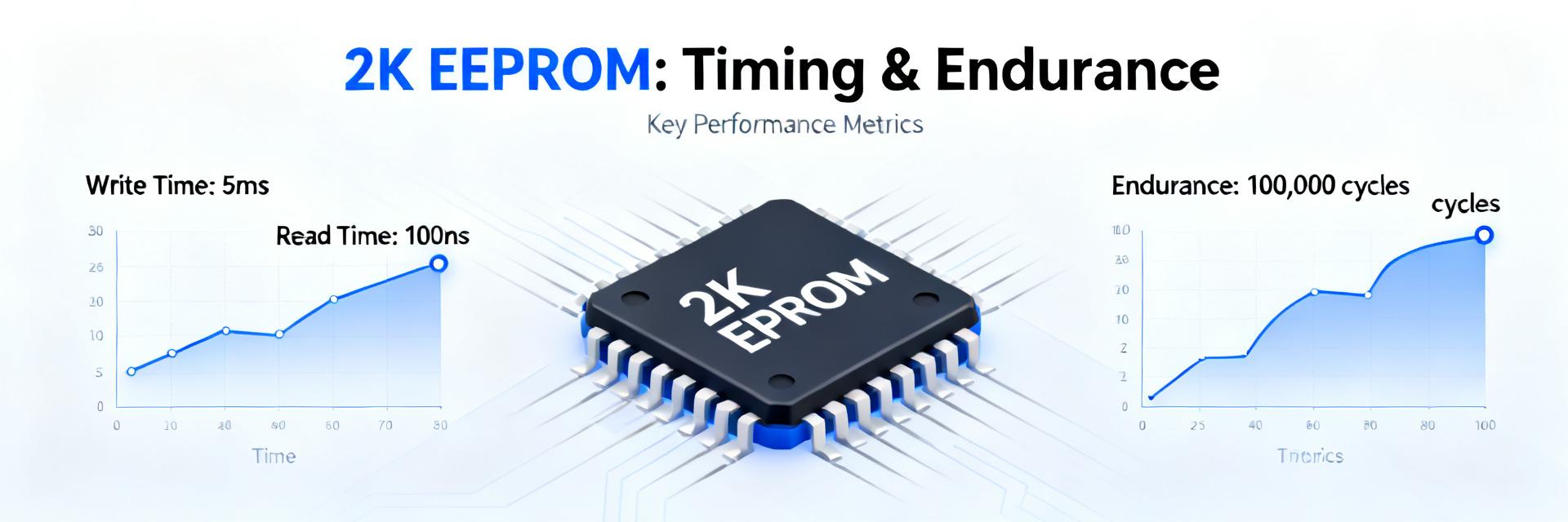
Point: Standby and active currents, retention period and write endurance define long‑term behavior. Evidence: Datasheet sections list IStandby, IActive, guaranteed data retention (e.g., years) and guaranteed write/erase cycles (endurance, typically specified as 10^4–10^6 cycles depending on grade). Explanation: Treat standby currents under a few microamps as low‑power; endurance above 100k cycles as robust for many embedded logs. Use these figures to set firmware write budgets and battery life models.
| Parameter | Standard Metric Value | System Integration Impact |
|---|---|---|
| Memory Capacity | 2 Kbit (128 words × 16-bit / 256 words × 8-bit) | Configured via ORG pin selection |
| Operating Voltage (VCC) | 1.8V to 5.5V | Supports standard low-voltage logic and 5V MCUs |
| Standby Current (ISB) | 1.5 μA (Max. @ VCC = 5.5V) | Ensures minimal power drain in idle sleep states |
| Write Cycle Time (tWR) | 4.0 ms (Max.) | Directly impacts non-blocking background tasks |
| Write Endurance | 1,000,000 Cycles / Word | Dictates wear-leveling & circular buffer structure |
| Data Retention | 100 Years (at Ta = +25°C) | Ensures reliable archival integrity of calibration data |
3 — Read/write behavior and timing breakdown (Method / test guide)
Typical write cycle mechanics and practical timing measurements
Point: A write sequence generally consists of command/address, data transfer, then an internal busy/write time. Evidence: The datasheet shows the command timing diagram and tWR for internal programming; logic analyzer traces reveal the device pull‑ups and acknowledge timing during tests. Explanation: Measure tWR by issuing a write, toggling appropriate control lines and capturing bus idle to idle; extended tWR indicates internal retries or voltage instability—log samples across temperature and VCC to verify.
Read modes, command timing and multi-byte operations
Point: Single‑word vs sequential reads differ in command overhead and bus usage. Evidence: The protocol section of the datasheet defines single‑read and sequential‑read behaviors and any required inter‑command delays or stop conditions. Explanation: Validate read timing by issuing single and sequential reads while capturing CS, CLK and data; verify throughput limits and ensure controller timing respects minimum inter‑command delays to avoid corrupted frames.
4 — Integration checklist: PCB, MCU interface and data integrity (Case / implementation)
Hardware wiring, pull-ups, and signal integrity
Point: Proper wiring and decoupling reduce communication errors. Evidence: Reference hardware diagrams indicate pull‑ups on open‑drain lines, local decoupling and short clock/data traces. Explanation: Place 0.1 μF decoupling close to VCC/GND pins, use modest pull‑ups on data lines per interface spec, and route clock/data as short differential‑like pairs where possible to limit ringing and cross‑talk.
Protection, wear‑leveling and fail‑safes
Point: Hardware and firmware safeguards extend lifetime and protect data. Evidence: Datasheets specify write‑protect inputs and brown‑out voltage thresholds; firmware patterns can distribute writes to avoid hotspots. Explanation: Implement write‑protect for critical regions, add brown‑out detection to suspend writes, and use simple circular buffers or page rotation to amortize writes across memory to delay wear‑out.
5 — Validation, procurement and troubleshooting checklist (Actionable recommendations)
How to validate datasheet claims in your lab
Point: A short validation matrix proves supplier claims and informs procurement. Evidence: Cross‑check supply currents, write timing, endurance and retention claims against measured samples using power meters, logic analyzers and accelerated write loops. Explanation: Measure IStandby and IActive across VCC range, log tWR/tACC on multiple parts, run repeated write cycles to sample endurance up to practical test limits, and record environmental stress results to confirm datasheet assertions.
Common failure modes and quick fixes
Point: Symptom→cause patterns speed troubleshooting. Evidence: Frequent issues include stuck writes, intermittent reads and address collisions, often traced to level mismatch, noisy VCC or bus contention. Explanation: Quick fixes: verify VCC and ground integrity, add/decrease pull‑up values, check chip select sequencing, and capture failing traces for escalation; retain failing sample logs and scope traces for vendor return support.
Summary
Point: The S-93A56B EEPROM balances modest capacity with predictable timing, endurance and low‑power tradeoffs. Evidence: Datasheet fields for tWR, tACC, retention and IStandby determine whether the part fits boot, configuration or logging roles. Explanation: Prioritize checking EEPROM specs in the datasheet against the validation checklist and run a brief lab matrix to confirm system suitability before bulk procurement.
Key summary
- The S-93A56B EEPROM matters most for its write‑cycle time and endurance; verify tWR and guaranteed write cycles in the datasheet to size write budgets and wear‑management strategies.
- Power and retention: confirm IStandby and retention guarantees to meet battery life and archival needs; low‑power typically means microamp standby currents and retention measured in decades.
- Integration checklist: follow wiring best practices, add decoupling and pull‑ups, implement write‑protect and brown‑out handling, and run the suggested lab validation before procurement.
Frequently Asked Questions
What EEPROM specs should I check first for embedded boot use?
Check read access time (tACC), interface speed limits and standby current first. Fast tACC reduces boot latency; interface clock limits determine throughput; low standby current protects battery‑backed systems. Cross‑verify these fields against the datasheet and measure with a logic analyzer for confirmation.
How do I validate write endurance claims from the datasheet?
Run accelerated write loops on representative samples, capturing error rates periodically. Correlate failures to cycle counts, ambient temperature and VCC. Use batch sampling to estimate variance; if endurance is critical, qualify parts to a fraction of datasheet cycles and implement firmware wear‑leveling.
What immediate steps fix intermittent read/write errors with this EEPROM?
First verify supply rails and decoupling, ensure correct pull‑ups and CS sequencing, and capture failing transactions with a scope. Short‑term fixes include stronger pull‑ups, reordering initialization, or increasing inter‑command delays; retain traces and part samples for escalation if hardware fixes fail.
What is the memory organization and interface structure of the S-93A56B?
The S-93A56B features a 2-Kbit capacity configurable in x8 (byte) or x16 (word) structure based on the ORG pin level. It relies on a 3-wire Microwire interface (CS, SK, DI, DO) to coordinate commands and capture high-reliability non-volatile configuration data.





