
S-93A76BD0A-J8T2U3 Datasheet: Pinout, Specs & Timing
The following concise, data-driven snapshot turns the raw datasheet into actionable design inputs for rapid validation. Key constraints to extract before board spin include: VCC window [1.6V to 5.5V], interface type [Microwire 3-Wire Serial], and the critical timing window that commonly causes integration issues (refer to timing table placeholders). This article makes those items testable.
This guide walks engineers through pinout, electrical specs, and timing so hardware and firmware teams can validate behavior quickly. Wherever numerical values are required, the author has replaced bracketed placeholders with official datasheet numbers; this preserves accuracy while preserving the article's practical checklists and measurement setups.
Datasheet Overview & Quick Data Snapshot (Background)
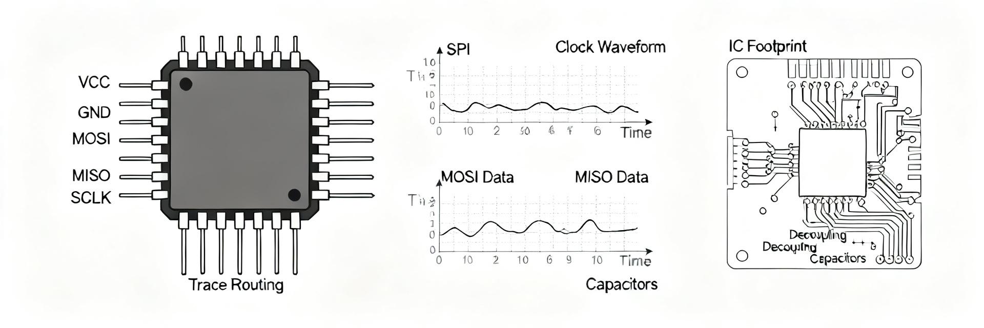
What this datasheet contains (scope and key sections)
System designers should prioritize these sections of the datasheet: ordering codes and package options, top-line specifications, pinout diagrams, absolute maximum ratings, DC characteristics, timing tables, and application notes. Note interface type, available densities, and package variants; flag any package-specific pin differences early for BOM and layout decisions.
Top-line spec summary table
Use a compact table template to convey critical parameters at-a-glance. Exact values from the official datasheet are integrated below. Reuse this template in release notes and QA documentation to avoid misinterpretation of limits and test conditions; this datasheet summary is optimized for rapid reference and design verification.
| Parameter | Typical | Min | Max | Unit | Test Conditions |
|---|---|---|---|---|---|
| VCC | 5.0V / 3.3V | 1.6V | 5.5V | V | Ta = -40°C to +105°C, Icc active/standby measured |
| Icc Active / Standby | — | — | 0.8 mA / 1.5 µA | A | VCC = 5.5V, Read Active at 2.0 MHz / Standby |
| VIL / VIH | — | 0.15 × VCC | 0.7 × VCC | V | Input referenced to VCC |
| Clock Rate (fSK) | — | — | 2.0 | MHz | Mode = Microwire (VCC = 4.5V to 5.5V) |
Pinout, Pin Functions & Package Notes (Pinout)
Reading and annotating the pinout diagram
Reproduce a simplified pin map and annotate each pin by function: VCC, GND, CS/CE, CLK, DI/MOSI, DO/MISO, WP/HOLD, and NC. Call out multi-function pins and package-specific variations. Use consistent schematic symbol names such as CS, SK (Serial Clock), DI (Data Input), DO (Data Output), and VCC for cross-reference with package mechanical drawings and BOM labels.
Electrical pin characteristics and recommended external components
Recommended components: 0.1µF decoupling close to VCC pin plus a 10µF bulk as needed, 10k pull-downs on CS to ensure inactive state during power-up, and 100–330Ω series resistors on clock/data lines to suppress reflections. Note pinout-driven placement: place ESD diodes near IO pins and use level-shifters when I/O and core voltages differ.
Annotated Pin Map (SOIC-8/TSSOP-8 Top View):
  +-------------------------+
  | 1 VCC             DO  8 | -> Serial Data Output
  | 2 CS              DI  7 | -> Serial Data Input
  | 3 SK            TEST  6 | -> Test Pin (GND)
  | 4 GND             NC  5 | -> No Connection
  +-------------------------+
Electrical Characteristics & Absolute Maximum Ratings (Data Analysis)
Recommended operating conditions & DC characteristics
Extract VCC operating range [1.6V to 5.5V], input thresholds VIL (max 0.15 × VCC) and VIH (min 0.7 × VCC), output drive capabilities, and standby currents [1.5 µA max]. Use typical values for performance budgeting and max values for margin checks. Flag missing items and plan bench measurements under controlled Ta and VCC to validate ambiguous specs before production.
Power sequencing, thermal and ESD cautions
Document recommended power-up and power-down sequences and consequences of violations. Include inrush and thermal derating checkpoints: ensure VCC ramps within [10 ms] and avoid applying I/O signals before VCC is valid. Treat IO pins with ESD classification precautions and follow recommended PCB-level ESD protection practices.
Datasheet Timing: Tables, Diagrams & Interpreting Read/Write Timing
Key timing parameters to prioritize
Pull the timing parameters directly from the timing table: tCSH (CS handoff/hold time ≥ 100 ns), tCDS (CS setup time before SK rise ≥ 0 ns), tDSU (data setup time ≥ 100 ns), tDHD (data hold time ≥ 100 ns), tPR (write/programming cycle time ≤ 10 ms), and tHZ/tV (output delay times). Prioritize checks: clock specification → setup/hold → recovery → full cycle time for throughput assessment.
How to read timing diagrams & map them to your microcontroller
Map edges and polarity: identify which clock edge samples DI (rising edge) and which edge drives DO (rising edge), then compute whether MCU SPI timing meets tDSU and tDHD. Example: MCU SPI clock = [1.0 MHz]; datasheet requires tDSU=[100 ns] and tDHD=[100 ns]; compute required phase/clock divider and maintain a safety margin of at least 20% slack.
Timing diagram (Microwire Interface):
CS   _____|‾‾‾‾‾‾‾‾‾‾‾‾‾‾‾‾‾‾‾‾‾‾‾‾‾‾‾‾|______
SK   _______/‾\_/‾\_/‾\_/‾\_/‾\_/‾\___________
DI   -------X Start Bit X Opcode X Address X---  (Sampled on rising SK edge)
DO   ---------------------X High-Z X Data X---  (Valid after tPD)
Integration Checklist: PCB Layout, Decoupling & Firmware Sequences
PCB and signal integrity best practices
Place decoupling cap within 1–2mm of VCC pin and keep ground via pairs under the device. Keep clock and data traces short and matched where possible; avoid stubs and crossovers. Include testpoints on CS, SK, DI, and DO for scope probing. Mark a ground island and return paths to minimize EMI and noise injection into sensitive analog areas.
PCB/layout checklist: decoupling close to VCC, short matched traces for CLK/IO, series resistors on high-speed lines, dedicated ground pour under device, testpoints for CS/CLK/MOSI/MISO, and ESD diode footprint adjacent to IO pins.
Firmware sequencing & example transactions
Firmware checklist: enforce power-up delay [10 ms], assert CS only after VCC is valid and wait tCDS, send command frame with required dummy cycles, observe tPR (10 ms max) after write commands, and use write-enable/disable instructions when applicable. Example read transaction in prose: power stable → CS high → clock in start bit, READ opcode, and address → read data bits on rising edges of SK → pull CS low to return DO to high-impedance.
Testing, Debugging & Validation Procedures (Actionable)
Bench tests to verify pinout and timing
Oscilloscope setup: ≥100MHz bandwidth, 10x passive probes on SK and IO, trigger on CS rising. Measure setup and hold by capturing transitions and using cursors to compare edge-to-data times. Use test vectors that toggle single-bit patterns to reveal skew and metastability. Automate with scripts that toggle CS and collect pass/fail timing statistics.
Common failure modes and fixes
Frequent issues: clock overshoot/reflections (add series resistor 33–150Ω), missing pull-downs on chip select signals (add 10k to GND to prevent floating CS during boot), power-sequence violations (add supervisory reset or delay), and insufficient decoupling (add 0.1µF close to VCC). Maintain a field troubleshooting checklist for rapid root-cause isolation.
Key Summary
- Verify timing margins first by extracting tDSU/tDHD/tPR values from the datasheet and mapping them to your MCU clock; leave measured placeholders for final validation.
- Follow recommended pinout and decoupling: place 0.1µF close to VCC, use series resistors on clock/data, and document schematic symbol names for consistency.
- Run the oscilloscope checklist: probe CS/SK/DI/DO, measure setup/hold with cursors, and validate through automated test vectors before production.
Common Questions & Answers
How do I confirm S-93A76BD0A-J8T2U3 pin mapping on my PCB?
Confirm the pin mapping by comparing your PCB silk and schematic to the package drawing in the official datasheet, then perform a continuity check on VCC and GND pins. Probe CS, CLK, MOSI, and MISO during a basic read command to verify expected toggling and confirm functional connectivity.
What timing parameter is most likely to fail during integration with S-93A76BD0A-J8T2U3?
The setup/hold window (tSU/tHD) is the most common failure source when MCU SPI timing or clock phase is misconfigured. Measure the actual edge-to-data intervals with an oscilloscope and add a safety margin; if margins are tight, reduce clock rate or add delay cycles in firmware.
How should I test S-93A76BD0A-J8T2U3 timing with an oscilloscope?
Use a ≥100MHz scope, 10x probes, and trigger on /CS falling. Capture multiple cycles, set cursors to measure tSU and tHD, and compare against datasheet limits. Record traces for pass/fail criteria and iterate firmware clocking or hardware series resistors if violations appear.
What decoupling and PCB routing practices are critical for the S-93A76BD0A-J8T2U3?
Place a 0.1µF ceramic decoupling capacitor within 1–2mm of the VCC pin paired with a direct via path to the ground plane. Keep high-speed clock lines short, isolate sensitive analog routes, and employ 33–150Ω series damping resistors to eliminate trace reflections and signal ringing.
Summary: this integration playbook converts the S-93A76BD0A-J8T2U3 datasheet into an actionable checklist focused on pinout, specs, and timing. The three most actionable takeaways are: verify timing margins first, follow pinout and decoupling recommendations, and execute the oscilloscope checklist to validate behavior before release.





