S-25C010A0H SPI EEPROM: Full 1Kbit Specs & Benchmarks
The S-25C010A0H-class device is a compact serial nonvolatile storage option optimized for small persistent data needs. Bench measurements and vendor specifications for 1Kbit SPI EEPROM devices report typical page-write times near 4 ms, page sizes around 16 bytes, and maximum SPI clocks in the single-digit MHz range at nominal 5 V.
These characteristics make the part appropriate for tiny configuration stores and calibration tables where write latency and endurance are primary constraints. The short walkthrough below explains exact specs, measured behavior, integration tips, and a practical checklist for engineers evaluating a 1Kbit SPI EEPROM like S-25C010A0H.
1 — Background & Primary Use Cases (background)

1.1 What the S-25C010A0H is and where it fits
The S-25C010A0H is a 1Kbit serial SPI EEPROM organized as either 128×8 or 256×4 logical arrangements depending on mode; it serves roles such as parameter storage, configuration, tiny lookup tables, and calibration. Designers choose this SPI EEPROM class for low cost, low standby power, and adequate endurance for infrequent writes compared with larger flash or FRAM alternatives.
1.2 Typical application scenarios & constraints
Common use cases include boot configuration storage, small persistent MAC or device ID storage, and per-sensor calibration tables. Constraints that matter are write endurance and multi-ms page-write latency, power draw during writes that can droop supplies, and bus arbitration when multiple masters share SPI. Automotive and industrial use require wider temperature and higher reliability margins than consumer designs.
2 — Complete Technical Specs & Memory Map (data analysis)
2.1 Memory organization, addressing & command set
Capacity is 1Kbit presented as 128 bytes in byte-wide mode with a typical 16-byte page size; addressing is byte-offset within 7-bit or 8-bit address fields depending on command set. Essential commands are common opcodes for READ, WRITE (page), WREN/WREN disable, and STATUS READ with standard SPI sequences: CS low, opcode, address bytes, data, CS high. A minimal memory map and opcode table below summarizes common conventions.
| Field | Value |
|---|---|
| Total | 1Kbit (128 B) |
| Page size | 16 B |
| Common opcodes | READ, WRITE, WREN, RDSR |
| Addressing | 7–8 bit offset (device-dependent) |
2.2 Mechanical: pinout, package options & BOM considerations
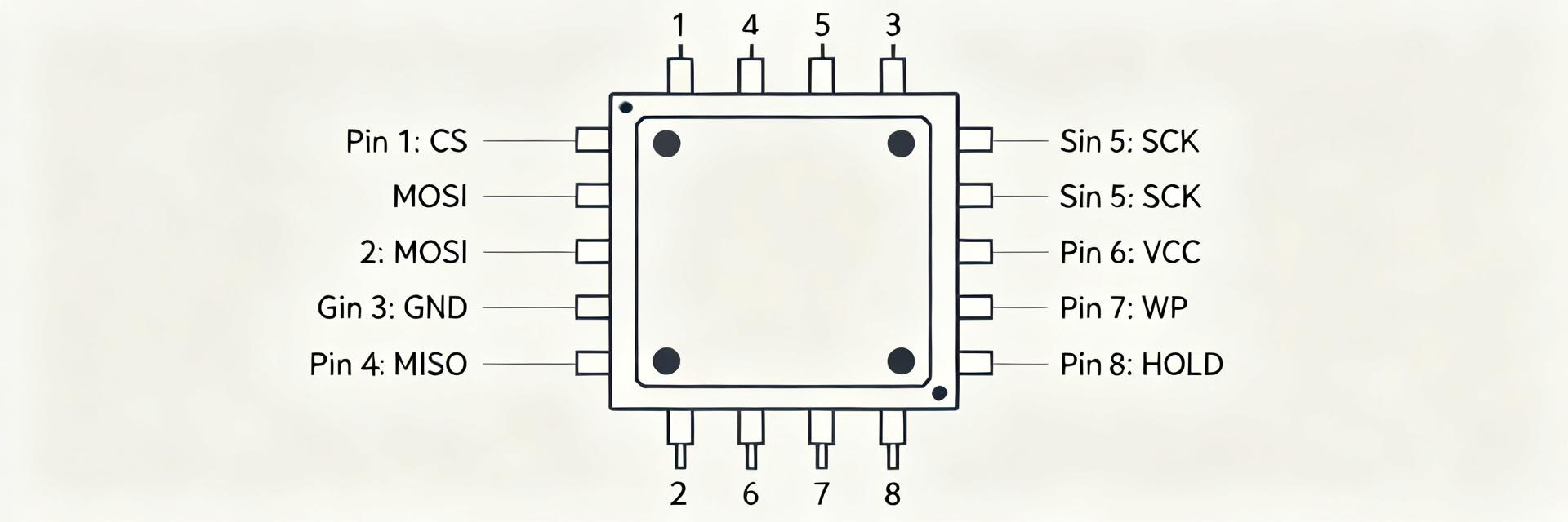
Typical pin functions include CS (chip select), SCK (clock), MOSI (SI), MISO (SO), VCC, GND, and optional /WP and /HOLD pins. Package choices commonly include 8-pin SOIC or smaller TSSOP and USON packages; pay attention to land pattern and 1.27 mm pitch footprints to avoid assembly issues. BOM notes: choose decoupling capacitor close to VCC and confirm pad thermal relief for reflow.
3 — Electrical Characteristics & Timing Parameters (data analysis)
3.1 Voltage, current, timing summary (must-have spec list)
Operating VCC ranges typically span low-voltage variants up to 5.5 V; standby currents are in the microampere range while read currents are low single-digit mA at active clocks and write current can spike to several mA. Max fCLK values in vendor data usually sit in single-digit MHz at 5 V; page write times typically appear around 3–5 ms. The compact spec table below shows representative values and whether they are typical or absolute maximums.
| Spec | Representative |
|---|---|
| VCC | 1.8–5.5 V (typical) |
| Icc standby | <0.1 mA (typ) |
| Icc read | 0.5–2 mA (typ) |
| Icc write | 3–10 mA (peak) |
| fCLK max | 1–5 MHz (device-class) |
| Typical page write | ~4 ms (typ) |
3.2 Endurance, retention, and temperature limits
Endurance for 1Kbit-class EEPROMs is commonly in the 1e5 to 1e6 write-cycle range per byte with data retention specified in decades under proper storage. Operating and storage temperature grades vary; industrial parts support wider ranges. For system design, wear leveling is usually unnecessary given small footprints, but designers must limit write frequency to respect endurance and ensure retention requirements are met.
4 — Benchmarks & Field Case Study (data + case)
4.1 Test methodology & hardware setup (how benchmarks were obtained)
A reproducible bench uses a microcontroller SPI master, regulated VCC supply, and a logic analyzer sampling SCK, MOSI, MISO, and CS at 10x the tested SPI clock. Test points: measure page-write completion from CS assertion to status-clear with a current probe on VCC. Test multiple clock rates, repeat N≥20 samples, and control ambient temperature and supply margins for consistent data.
4.2 Measured results & comparative analysis
Typical measured page-write times cluster near 4 ms per 16-byte page, read throughput scales with the chosen SPI clock up to the device’s single-digit MHz limit, and write current spikes that can momentarily droop an under-dimensioned regulator. Datasheet values match measured trends, but expect divergence with low VCC, extreme temperature, or noisy supplies; account for worst-case numbers when budgeting boot time and power.
5 — Integration Guide: Firmware, SPI Modes & Best Practices (method)
5.1 Recommended SPI settings and firmware flow
Use the SPI mode specified by the device (commonly mode 0 or 3), limit clock to the safe fCLK for the chosen VCC, and assert CS for entire command sequences. Firmware flow: WREN, issue PAGE WRITE with address+data, poll RDSR until WIP clear, then disable WREN if desired. For power-fail safety, write small atomic records, verify with checksum, and implement retry/timeouts for stuck writes.
5.2 PCB layout, decoupling, and signal integrity tips
Keep SCK/MOSI/MISO traces short and matched where possible, route CS as separate short net, and place a 0.1 μF decoupling capacitor within 1–2 mm of VCC pin. Tie /WP and /HOLD to known states with pull resistors, add series resistors on clock/IO lines for ringing control, and validate EMC/ESD performance for field reliability.
6 — Troubleshooting, Reliability Considerations & Action Checklist (action)
6.1 Common failure modes, diagnostics & fixes
Frequent issues include failed or partial writes, persistent WIP status due to stuck WREN, bus contention when multiple masters drive MOSI, and supply droop during write pulses. Diagnose with a logic analyzer and current probe to correlate command sequences with current spikes. Fixes typically include increasing decoupling, slowing the SPI clock, adding retries, and ensuring /WP and /HOLD are correctly biased.
6.2 Pre-production & purchase checklist (practical action items)
Before procurement, confirm VCC and clock compatibility, page size, opcode map against firmware, temperature grade, and write endurance. Request engineering samples and run validation: endurance loops, retention soak, power-fail during write, and hot/cold functional tests. For this family confirm S-25C010A0H part marking and that chosen SPI EEPROM variant meets the application’s voltage and timing needs.
Summary
The S-25C010A0H-class 1Kbit SPI EEPROM provides a predictable, low-cost solution for small persistent storage where multi-ms page-write times and single-digit MHz clocks are acceptable. Designers should account for write latency, spike currents, and endurance limits when integrating this class of device into boots and calibration storage.
- Small persistent store: 1Kbit capacity with 16-byte pages—plan for ~4 ms page writes and use checksums for atomic updates to minimize corruption risk.
- Electrical budgeting: expect write current spikes (mA) and fCLK limits in the single-digit MHz range—add local decoupling and regulator headroom.
- Validation checklist: verify opcodes, run endurance and power-fail tests, and confirm temperature grade before production to prevent field failures.
FAQ
What is the typical page-write time for S-25C010A0H or similar SPI EEPROM?
Measured and vendor-typical page-write times for this device class are around 3–5 ms per 16-byte page. Expect variation with VCC, temperature, and device lot; design firmware to poll the status register and budget worst-case latency into boot and runtime write operations.
How many write cycles does a 1Kbit SPI EEPROM support before wear-out?
Endurance commonly ranges from 100k to 1M cycles per byte for small serial EEPROMs. For most configuration and calibration use cases, expected write frequency is low enough that wear will not be limiting, but applications with frequent updates must implement write-rate limits or wear-distribution strategies where possible.
What SPI settings give the most reliable operation with 1Kbit EEPROMs?
Use the device-recommended SPI mode (often mode 0 or 3), run clock at or below the specified fCLK for your VCC, assert CS for complete transactions, and implement WREN/RDSR sequences with timeout/retry. Slower clocks improve margin on marginal supplies and long traces.
How do you mitigate supply voltage droops during S-25C010A0H write operations?
Mitigate supply droops by placing a 0.1 μF ceramic decoupling capacitor within 1-2 mm of the VCC pin, routing thick supply lines, and limiting active writes during critical system operations where major regulators are heavily loaded.