S-35190AH-J8T2U Complete Datasheet Summary & Key Specs
The S-35190AH-J8T2U is a low-power real-time clock IC optimized for battery-backed systems, specified for 1.3–5.5 V operation and guaranteed across a wide temperature range. This summary highlights the device’s electrical envelope—operating voltage 1.3–5.5 V, typical timekeeping current ~1.2–1.4 µA at mid-voltage, and operating temperature −40 °C to +105 °C—so engineers can quickly assess suitability for embedded designs. S-35190AH-J8T2U appears throughout the technical discussion below.
Designed for compact PCB implementations, the part balances minimal standby current with robust VBAT switchover behavior and a simple 3-wire serial interface. The following sections distill package, electrical limits, performance trends, interface timing, integration best practices, example use cases, and a procurement/testing checklist for rapid prototyping and qualification.
1 — S-35190AH-J8T2U: Product Overview & Electrical Highlights

The device is positioned as a small-package RTC for battery-backed applications with low quiescent draw and industrial temperature tolerance. Key electrical highlights include a supply window from 1.3 V to 5.5 V, VBAT backup support, single-digit microampere timekeeping current, and standard CMOS I/O levels compatible with common microcontrollers. Designers should review absolute maximum ratings and recommended operating conditions before layout and part selection.
Package & pinout snapshot (datasheet reference)
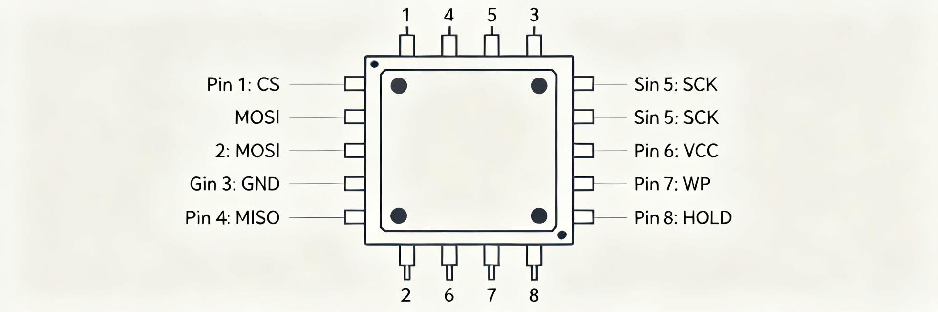
Available in SOP-8 and TSSOP-8 style packages (check the specific ordering code for the mechanical variant). Pin functions include power (VCC, VBAT), ground, serial clock, data, chip enable, and an open-drain interrupt/OUT pin. Recommended PCB footprint guidance in the full datasheet shows typical land pattern, pad-to-pin clearances, and thermal pad suggestions; include exposed pad routing and consistent silkscreen for orientation. A concise pin table should be placed beside the footprint during PCB review for quick reference.
Key electrical specs at a glance
Absolute and recommended values to note: supply range 1.3–5.5 V; VBAT behavior supports seamless switchover to backup cell; typical timekeeping current ~1.2–1.4 µA (mid-voltage), with higher values near supply extremes; I/O drive is limited—plan external buffering if driving large loads. Max ratings include absolute voltage and junction temperature limits; ensure margin for transient events and avoid exposing VBAT to charging sources without proper protection.
| Parameter | S-35190AH-J8T2U Spec Value | Design Notes / Operating Conditions |
|---|---|---|
| Operating Supply Voltage | 1.3 V to 5.5 V | Supports direct operation from main rail or lithium backup cells. |
| Timekeeping Current | 1.2 µA to 1.4 µA (Typical) | Measured at mid-voltage; design for higher limits at elevated temperatures. |
| Operating Temperature | −40 °C to +105 °C | Qualified for harsh industrial environments and cold-start profiles. |
| Serial Interface | 3-Wire (CE, CLK, DATA) | Requires careful firmware control for setup, hold, and clock speeds. |
| Package Styles | SOP-8 / TSSOP-8 | Compact footprint optimized for high-density modern PCB assemblies. |
2 — S-35190AH-J8T2U Performance Data & Operating Ranges
Performance is dominated by supply level and temperature. Timekeeping current rises at lower supply and high temperature, and oscillator stability follows typical crystal behavior; plan worst-case budgeting for battery life and thermal derating. The datasheet contains detailed curves; use those to extrapolate battery lifetime under intended duty cycles and wake intervals.
Voltage, current, and temperature performance
Typical timekeeping current stated near mid-supply is ~1.2–1.4 µA; at 1.3 V and elevated temperatures the current can increase noticeably. Decoupling (0.1 µF close to VCC and a larger 1–10 µF bulk cap) is recommended to suppress ripple; the oscillator is sensitive to supply noise—place caps within 1–2 mm of the device. For thermal derating, assume higher leakage and validate timekeeping over the full −40 °C to +105 °C range in chamber tests.
Accuracy, drift, and oscillator behavior
Frequency accuracy is governed by the chosen 32.768 kHz crystal/resonator and its load capacitance; expect ppm-level drift that varies with temperature and aging. Characterize in-system accuracy using long-duration sample logging and compare against a GPS-disciplined reference or lab timebase. Record-startup time and frequency settling during power cycles to understand time-to-valid after VBAT switchover.
3 — Interface, Command Flow & Timing (3-wire RTC)
The S-35190AH-J8T2U uses a simple 3-wire serial protocol (CLK, DATA, CE), with a small set of read/write commands for time, control registers, and alarms. Command transactions are short; implement retries and status checking in your driver to handle transient noise or bus contention.
3-wire serial protocol overview
Typical command flow: assert CE, shift out command and address on DATA synchronized to CLK, then read or write register bytes LSB-first. Maintain proper setup and hold times and respect the maximum clock frequency from the timing table—overspeeding increases error risk. Provide a timing checklist for firmware: CE setup, MOSI timing, MISO sampling edge, and CE hold after the final bit.
VBAT switchover and backup behavior
VBAT switching is automatic; however, external diode or ideal diode arrangements can protect backup cells from reverse currents. Test VBAT behavior by inducing brown-out on VCC and monitoring register retention and interrupt outputs. Verify failure modes: rapid VCC cycling, partial voltage drops, and cold-crank scenarios to ensure clean VBAT handover without register corruption.
4 — Integration & Design Best Practices
Layout and power design materially affect RTC reliability. Keep analog and digital grounds separate locally and tie to a single point; place decoupling close to VCC and add a dedicated ground island for the crystal area. Minimize noisy traces near the crystal and VBAT route.
Power supply, decoupling, and PCB layout tips
Use a 0.1 µF ceramic in parallel with a 1 µF–4.7 µF low-ESR cap at VCC; route ground return directly to the device’s ground pin. Provide a test point on VBAT and VCC for current measurement and monitoring. Keep the crystal traces short and symmetric and avoid vias in the oscillator loop if possible.
Crystal/oscillator selection and noise mitigation
Choose a 32.768 kHz crystal with recommended load capacitance (per crystal vendor data). Leave a keep-out zone for high-frequency switching regulators and noisy clock lines; if required, add small RC filtering on supply or ferrite beads to reduce conducted noise. Verify oscillator start-up time and amplitude on prototype boards.
5 — Typical Use Cases & Example Configurations
Typical deployments include battery-backed data loggers, telematics units, and industrial controllers needing persistent time across power loss. The wide voltage and temperature range make the part suitable for automotive and industrial environments when combined with appropriate backup cell and supply conditioning.
Application examples and configuration variants
Common configurations: single-supply microcontroller-hosted RTC; VCC with coin-cell VBAT for backup; and buffered outputs driving interrupt inputs on host CPUs. Select the VBAT cell capacity based on worst-case timekeeping current and expected lifetime between replacements or recharges.
Firmware snippets & register access patterns (pseudo)
Pseudocode: initialize CE low, configure control registers, poll oscillator-ready bit, read time registers via sequential read commands, convert BCD fields to binary, and schedule host wake intervals. On power transitions, use guarded write sequences and verify register reads post-switchover to avoid corruption.
6 — Quick Checklist: Key Specs, Testing & Procurement Guidance
Use this section as a compact reference for procurement and quick validation before board commit. Confirm markings and package variant on incoming reels and cross-check lot traceability before assembly.
Printable quick-reference spec checklist
- Supply range: 1.3–5.5 V — VBAT support for backup (design for safe switchover)
- Timekeeping current: ~1.2–1.4 µA typical — budget for worst-case thermal/voltage increases
- Temperature range: −40 °C to +105 °C — validate across intended environment
- Package/pinout: SOP-8 / TSSOP-8 variants — confirm footprint and pin mapping
- Crystal: 32.768 kHz recommended — follow load capacitance guidance
Qualification, testing, and ordering checks
Incoming test items: pin continuity and orientation, oscillator start-up, VBAT switchover behavior, and timekeeping stability at temperature extremes. For procurement, verify part marking and datasheet revision on the device label, and require lot traceability for critical programs.
Summary
For low-power, wide-temperature RTC needs the S-35190AH-J8T2U delivers a practical balance of minimal timekeeping current, broad supply range, and VBAT backup capability. Use the quick spec checklist and layout/firmware tips above to accelerate prototype validation; consult the full datasheet for register maps and detailed timing to finalize production firmware and test plans. This summary emphasizes the main datasheet points and key specs for rapid evaluation.
What is the operating voltage range of S-35190AH-J8T2U?
The S-35190AH-J8T2U supports a wide supply voltage range from 1.3 V to 5.5 V, optimizing it for battery-backed and low-power systems.
What is the typical timekeeping current consumption?
It features extremely low current consumption, typically around 1.2 to 1.4 µA at mid-voltage, though it may increase near temperature/voltage extremes.
What interface protocol does S-35190AH-J8T2U use?
It uses a standard 3-wire serial interface (consisting of CE, CLK, and DATA lines) for command, control, and timekeeping register communication.
What is the operating temperature range?
The device is rated for industrial operations spanning from −40 °C to +105 °C, making it suitable for demanding industrial and automotive applications.