
S-93A86BD0A Datasheet: Pinout & Electrical Specs Overview
The S-93A86BD0A is a 16-Kbit serial EEPROM class device commonly used for nonvolatile configuration, calibration and small data logging. Typical electrical specs for quick reference: VCC range 2.5–5.5 V, serial clock up to ~2 MHz, and a typical write cycle time ~4 ms. This datasheet summary highlights pinout, key electrical specs and integration tips so designers can map requirements into prototypes quickly; note the device label S-93A86BD0A-T8T2U3 is used here as a typical ordering example and must be verified against the official datasheet.
(1) Background & Device Overview — Background introduction type
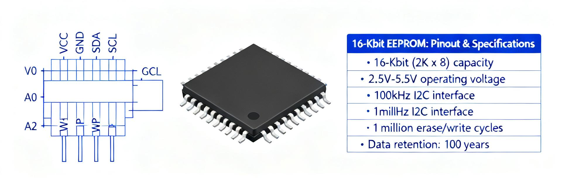
Device class and intended applications
This device is a Microwire / 3‑wire serial EEPROM offering 16 Kbit organization (typically arranged as 2048 x 8 bits or equivalent device organization noted in the official datasheet). Designers select this 3‑wire serial EEPROM for compact nonvolatile storage of configuration bytes, calibration constants and occasional event logs because of small footprint, low standby current and simple MCU interface. Addressing is word-based; verify MSB/LSB order in the official datasheet for correct addressing and page boundaries.
Ordering codes & package options (package names generically)
Common package formats include 8-pin SOP (SOP‑8), 8-pin SOIC/DIP-style outlines and small plastic leaded packages; suffixes usually indicate package and temperature grade. Package selection affects PCB footprint, thermal dissipation and assembly choice: SOP-8 gives smaller board area, dual‑row or through‑hole variants ease prototyping. Always confirm land pattern and thermal derating notes in the official datasheet for the chosen package option.
(2) Pinout Detailed Breakdown — Data analysis type
Pin map & functional descriptions
Typical pin set: CS (chip select / chip enable), SK (serial clock), DI (data in / SI), DO (data out / SO), VCC (power), VSS/GND, WP (write protect) and any NC/reserved pins. Idle levels: CS high = device deselected (or as specified), SK idle low; DI/DO require defined input thresholds. Use pull‑ups on DO when bus shared and enable WP high/low per datasheet to prevent writes. Confirm exact pin numbers per package variant in the official datasheet.
Pin-level usage tips & PCB footprint notes
Route SK and DI/DO as short, matched-length traces where possible; place a 22–100 Ω series resistor at the SK and DI pins to limit ringing. Place a 0.1 µF ceramic decoupling capacitor adjacent to VCC and VSS pins. If using SOP-8 or similar, confirm land pattern tolerances and avoid thermal relief under the part if not required; NC pins should be left unconnected unless the datasheet specifies otherwise.
(3) Electrical Specifications & Operating Conditions — Data analysis type
DC characteristics (voltage, current, thresholds)
Key DC parameters (typical example, confirm official datasheet): recommended operating VCC range 2.5–5.5 V; absolute max VCC typically VCC + 0.5 V negative limits to VSS −0.5 V; standby supply current in the nA–µA class; active supply current during clocked reads in the µA range; during internal write cycles device current spikes to several mA—design regulators accordingly. Input leakage, VOH and VOL thresholds follow standard CMOS levels; always refer to the official datasheet absolute max vs recommended ranges before production.
| Parameter | Typical / Nominal | Max / Notes |
|---|---|---|
| VCC operating | 2.5–5.5 V | Absolute max VCC ±0.5 V over/under |
| Standby current | ~1–10 µA | Varies by temperature / package |
| Write-cycle current | ~5–10 mA peak | Transient during tWR |
| Input leakage | ±1 µA typical | Spec table for IO pins |
AC/timing characteristics (clock, read/write timing)
Timing constraints drive throughput: maximum SK clock typically ~2 MHz (typical example); minimum pulse widths and setup/hold times are critical for reliable reads. Typical write cycle time (tWR) is ~4 ms; internal write recovery (tREC) must be observed before next operation. CS timing governs command framing—observe tCSS, tCSH (chip select setup/hold) values. These timing numbers limit sustained transfer rates and affect MCU ISR timing and DMA strategies.
| Timing | Typical | Max / Notes |
|---|---|---|
| fSK (max) | ~2 MHz | Lower at high temp or certain voltage |
| tWR (write cycle) | ~4 ms | Up to tWR(max) in spec; poll for completion |
| tREC (internal recovery) | -- | Observe before next write |
(4) Integration & Design Guidelines — Method guide type
Power supply, decoupling and level-translation
Place a 0.1 µF ceramic decoupler within 1–2 mm of VCC and VSS pins, with a 1 µF bulk capacitor on the local rail for write‑current transients. If MCU IO uses different VCC, use unidirectional level shifters or open‑drain with pull‑ups sized to meet input rise-time specs. Size the regulator to handle peak write-cycle current (~several mA) plus margin; monitor VCC droop during writes on first prototypes.
Signal integrity, bus arbitration & write-protect handling
To minimize ringing on SK/DI/DO, add small series resistors and avoid long stubs; keep clock trace impedance controlled. If multiple devices share DI/DO, use tri‑state outputs or dedicated chip selects; ensure only one DO drives the bus. Use WP as recommended by the official datasheet to disable programming during production or critical runtime; verify WP polarity and implement pull resistors per application needs.
(5) Interfacing Example: Microwire Read/Write Sequence — Case showcase type
Typical read sequence (step-by-step)
Read flow (pseudocode/bullets): 1) Assert CS active (per datasheet polarity). 2) Send the start/opcode bits and address MSB→LSB. 3) Toggle SK for address and data clocks at allowed timing (observe setup/hold). 4) Release DI and sample DO on the specified clock edge. Common pitfalls: off‑by‑one addressing, wrong bit order, CS timing violations. Confirm with timing diagram and test vectors.
Example (abstract):
CS = ACTIVE
send_bits(opcode + addr MSB..LSB) // observe t_setup
for i = 0..7: toggle(SK); read_bit = sample(DO)
CS = INACTIVE
Typical write sequence & endurance considerations
Write flow: 1) Assert CS, transmit write opcode + address, then send data bytes. 2) After data, deassert CS if required to initiate internal tWR; device performs internal programming (tWR ~4 ms typical). 3) Poll device or read back to verify completion. Endurance: typical EEPROM write endurance is in the 10^4–10^6 cycle range—design wear‑leveling or limit write frequency for system durability.
(6) Validation Checklist & Troubleshooting — Action recommendations type
Quick validation tests and expected measurements
First‑power checklist: confirm VCC to VSS continuity and correct rail voltage (2.5–5.5 V). With CS inactive expect DO to be tri‑stated or pulled per board design. Measure VCC under idle and during a write cycle to verify regulator margin; observe SK pulse widths and fSK with oscilloscope at pin SK. Perform a basic read-back of a known location to confirm addressing and timing.
Common failure modes and fixes
No response: check VCC, CS polarity, and pull resistors. Corrupted data: verify clock timing, DI bit order, address boundaries and decoupling. Write fails: ensure WP not asserted, confirm tWR and allow internal recovery, and check for bus contention. Use stepwise isolation: single‑device test jig, bench MCU toggling, and oscilloscope capture of CS/SK/DI/DO to triage.
Summary & Next Steps
Recap: confirm pinout essentials (CS, SK, DI, DO, VCC, VSS, WP), check critical electrical specs (VCC range 2.5–5.5 V, tWR ~4 ms typical, max clock ~2 MHz) and apply integration tips such as 0.1 µF local decoupling and series resistors on SK. Before production, verify all numeric values in the official datasheet; test first prototypes using the validation checklist and observe write current transients for regulator sizing. The S-93A86BD0A and datasheet guidance are the authoritative references for final sign-off; when quoting the exact ordering string S-93A86BD0A-T8T2U3 confirm variant-specific limits in the datasheet.
- Pinout priority: validate CS polarity and WP function before functional tests; check DI/DO direction and pull-ups when sharing buses with MCUs or multiple devices.
- Power and timing: ensure VCC within 2.5–5.5 V, include 0.1 µF decoupling near VCC, and budget for tWR (~4 ms) in firmware state machines.
- Signal integrity: route SK and data traces short, add small series resistors, and use bus arbitration or tri‑state buffering for multi‑drop configurations.
FAQ: common S-93A86BD0A questions
Q1: How do I wire S-93A86BD0A to an MCU using Microwire?
Wire CS to a dedicated GPIO configured as chip select; SK to a GPIO or SPI SCLK; DI to MOSI-equivalent and DO to MISO-equivalent. Ensure MCU IO levels match VCC or use level translation. Observe SK timing and CS framing per the official datasheet; include 0.1 µF decoupling and series resistors to improve signal integrity.
Q2: What electrical specs should I prioritize from the datasheet?
Prioritize VCC operating range (2.5–5.5 V typical example), absolute maximum ratings, tWR (write cycle time), and max clock frequency. Also check peak write current for regulator sizing and IO threshold levels if interfacing with different-voltage MCUs. Confirm all values in the official datasheet for your selected package and temperature grade.
Q3: How can I verify a write completed successfully on the 3-wire EEPROM?
Two common methods: 1) Polling — attempt a read or send a status poll sequence until the device responds, indicating internal write complete; 2) Read-back verification — read the written address and compare bytes. Always wait at least the datasheet’s tWR or use the device’s busy/poll mechanisms to avoid corrupting data.
Q4: What are the common failure modes of the S-93A86BD0A and how do I fix them?
Common issues include no response (check VCC, CS polarity, pull resistors), data corruption (verify clock timing, DI bit order, address boundaries, decoupling), and write failures (check WP pin status, verify tWR, ensure no bus contention).





