
S-25C020A0H-K8T2UD datasheet: full pinout & specs guide
The S-25C020A0H-K8T2UD-focused guide extracts the most used metrics engineers need to integrate a small serial NOR flash into embedded and IoT designs. This article prioritizes the practical values from the datasheet so teams can move faster through schematic, PCB layout, firmware bring-up, and validation without wading through descriptive text. Expect pin maps, electrical limits, timing guidance, PCB and firmware checklists, and troubleshooting steps.
1 — At-a-glance: S-25C020A0H-K8T2UD quick spec summary (background)
Product identity in one line: S-25C020A0H-K8T2UD serial NOR flash, SPI-compatible small-capacity device suitable for boot and configuration storage. This compact device typically offers low-power operation, a single- or quad-SPI interface variant, and endurance/retention characteristics targeted at code store and infrequent update workloads — see the compact specs table below for quick design-facing numbers.
1.1 — One-line product identity & key specs
Key specs here oriented for selection and BOM notes: capacity, package, voltage domain, interface, and typical endurance/retention. These values represent the dataset engineers most commonly copy into part-parameter sheets when preparing footprints and electrical constraints for system validation.
| Parameter | Value |
|---|---|
| Density | 2 Mbit (256 KB) |
| Package options | 8-pin SOP / WSON variants |
| Supply voltage | 2.7–3.6 V |
| Interface | SPI (standard / fast modes) |
| Operating temp | -40 °C to +85 °C |
| Endurance / Retention | Typical: 100k cycles / 20+ years |
1.2 — Typical use cases and differentiators
Common uses: boot code storage, configuration NVRAM, small filesystem blocks, and IoT firmware snapshots. Differentiators include minimal power footprint, small PCB area, simple SPI command set, and low-cost availability. Pick this part when capacity and fast random-read performance at low power trump large erase granularity or high sustained write throughput.
2 — Full pinout: pin map & per-pin descriptions (data-driven)
Below is a concise pinout and per-pin behavioral summary to accelerate schematic capture and footprint verification. The table and notes prioritize signals engineers probe during bring-up and highlight idle states and recommended pull directions for reliable bus sharing and hot-plug scenarios.
2.1 — Pin map graphic + table
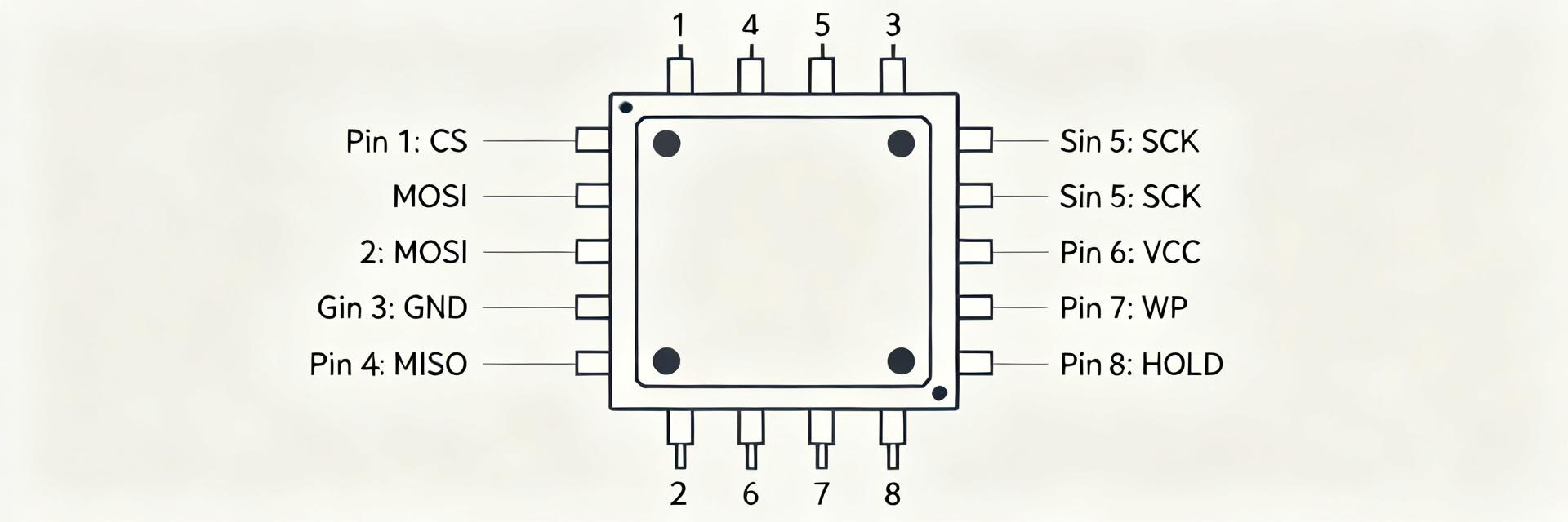
The pin map follows a top-view 8-pin layout typical of small serial flash packages; pins include CS, CLK, MOSI, MISO, VCC, GND, WP/HOLD. Use the table to verify each net before first power-up and to create testpoints for scope/probing of clock and data signals.
| Pin # | Name | I/O type | Default / Notes |
|---|---|---|---|
| 1 | CS | I | Active low; pull‑up recommended |
| 2 | CLK | I | Input; keep short trace |
| 3 | MOSI (SI) | I | Input during commands |
| 4 | GND | PWR | Connect to clean ground plane |
| 5 | MISO (SO) | O | Tri‑state when CS high |
| 6 | WP/HOLD | I | Optional pull‑up; timing-sensitive |
| 7 | VCC | PWR | 2.7–3.6 V; decouple close |
| 8 | NC/Reserved | — | Do not connect if NC |
2.2 — Detailed pin electrical behavior and recommended usage
CS: active low, must be high to release MISO. CLK: CMOS input, edge rates matter—keep series resistor if ringing. MOSI: drive-strength from MCU; avoid contention. MISO: tri‑state when idle. WP/HOLD: recommended pull‑ups to VCC (100 kΩ) unless used. RESET sequences: assert per datasheet timing before issuing commands.
3 — Electrical characteristics & timing specs (data deep-dive)
3.1 — DC characteristics & absolute maximum ratings
Design for recommended operating conditions, not absolute maxima. Typical VCC: 2.7–3.6 V; absolute max clamp at VCC + 0.3 V. Standby current is low (µA range) while active current rises with clock and I/O activity. Specify decoupling: 0.1 µF close to VCC and a 1 µF bulk cap on board to stabilize supply for transient program/erase events.
3.2 — Timing parameters, command latency & throughput
Clock frequency: device supports standard and fast SPI clock rates up to specified max; conservative firmware should target 20–50% below rated max for margin. Typical page program times are in millisecond range; sector erase can be tens to hundreds of milliseconds. Implement status‑bit polling with timeout margins (x1.5–2 of typical tprog) rather than fixed delays.
4 — Integration & design best practices (method/guide)
4.1 — PCB layout, footprint & power decoupling
Keep CLK/MOSI/MISO/CS traces short and with controlled impedance where possible. Place 0.1 µF decoupling within 2–3 mm of VCC pin; add a 1 µF bulk cap nearby. Provide a solid ground plane, thermal vias if package needs heat spread, and an ESD protection diode network on IOs if assembly experiences handling risk.
4.2 — Interface & firmware integration (command sequences)
Bootflow: ensure VCC ramp and reset sequencing complete before issuing commands. Typical sequence: CS low → Send Read ID / Read Status → poll SR[BUSY] until clear. Use Write Enable before any program/erase. Pseudocode should poll status with exponential backoff and a hard timeout to avoid infinite waits.
5 — Testing, troubleshooting, procurement & alternatives (action)
5.1 — Validation & debug checklist
Checklist: verify VCC/GND continuity and correct voltage; confirm CS polarity; probe CLK/MOSI/MISO for expected toggles on ID read; verify status register changes after WREN and program operations. When Read ID fails, check pull‑ups, CS wiring, and reset sequencing first. Keep a minimal test script that performs ID, read, program, and verify cycles.
5.2 — Sourcing, footprint compatibility & drop-in alternatives
When selecting alternatives, compare capacity, VCC range, IO voltage tolerance, supported SPI modes, and erase/program granularity. Prefer pin-compatible parts with similar timing envelopes to minimize firmware changes. Account for procurement lead time and lot-to-lot marking differences when qualifying a replacement.
Summary
- The S-25C020A0H-K8T2UD datasheet distills essential specs and constraints engineers need for schematic and firmware — capacity, VCC range, package, and endurance are primary selection drivers.
- Pinout essentials: verify CS polarity, CLK integrity, and recommended pull‑ups on WP/HOLD; ensure decoupling and short traces for reliable SPI transactions.
- Timing & reliability: implement status‑bit polling with conservative margins and avoid relying on single fixed delays for program/erase completion.
FAQ
What is the S-25C020A0H-K8T2UD pinout and how do I verify it?
Confirm pin mapping against the part marking and schematic: check VCC and GND first, then probe CS, CLK, MOSI, and MISO with a scope while issuing a Read ID command. If no activity appears, re-check CS polarity and any pull‑ups on WP/HOLD or RESET lines. Use a minimal MCU test script to toggle CS and clock to validate connectivity.
How should firmware handle S-25C020A0H-K8T2UD timing and busy polling?
Use Read Status Register polling instead of fixed delays. After issuing program/erase, poll the BUSY bit and apply a conservative timeout (for example, 1.5–2× the typical program time). Back off polling frequency progressively to reduce bus traffic and CPU usage, and always include a hard failure path to recover from stuck states.
What are practical PCB layout tips for S-25C020A0H-K8T2UD integration?
Place the device close to the MCU or SPI controller, keep high-speed traces short, add series resistors for signal integrity if needed, and place a 0.1 µF decoupling capacitor within millimeters of VCC. Route MOSI/MISO away from noisy switching nets and ensure a contiguous ground plane under the flash device for stable reference and thermal performance.
What are recommended pull-up resistor values for WP/HOLD and CS?
Typically, 10 kΩ to 100 kΩ pull-up resistors connected to VCC are recommended on CS and WP/HOLD pins. This maintains stable high levels during micro-controller reset and prevents accidental write cycles or bus suspension during power transitions.





